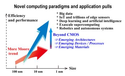
Beyond CMOS on:
[Wikipedia]
[Google]
[Amazon]
Beyond CMOS refers to the possible future  CMOS devices sizes continue to shrink – see Intel's process–architecture–optimization model (and older
ITRS 2013 edition
*
EMERGING RESEARCH DEVICES SUMMARY
*
Process Integration, Devices and structures summary
Electronic design Digital electronics Logic families Integrated circuits
digital logic
A logic gate is a device that performs a Boolean function, a logical operation performed on one or more binary inputs that produces a single binary output. Depending on the context, the term may refer to an ideal logic gate, one that has, for ...
technologies beyond the scaling limits of CMOS
Complementary metal–oxide–semiconductor (CMOS, pronounced "sea-moss
", , ) is a type of MOSFET, metal–oxide–semiconductor field-effect transistor (MOSFET) semiconductor device fabrication, fabrication process that uses complementary an ...
technology. which limits device density and speeds due to heating effects.
''Beyond CMOS'' is the name of one of the 7 focus groups in ITRS 2.0 (2013) and in its successor, the International Roadmap for Devices and Systems.
CPUs using CMOS were released from 1986 (e.g. 12 MHz Intel 80386
The Intel 386, originally released as the 80386 and later renamed i386, is the third-generation x86 architecture microprocessor from Intel. It was the first 32-bit computing, 32-bit processor in the line, making it a significant evolution in ...
). As CMOS transistor dimensions were shrunk the clock speeds also increased. Since about 2004 CMOS CPU clock speeds have leveled off at about 3.5 GHz.
 CMOS devices sizes continue to shrink – see Intel's process–architecture–optimization model (and older
 tick–tock model
Tick–tock was a production model adopted in 2007 by integrated circuit, chip manufacturer Intel. Under this model, every new process technology was first used to manufacture a die shrink of a proven microarchitecture (tick), followed by a new mic ...
) and ITRS:
* 22 nanometer
The "22 nm" node is the process step following 32 nm in CMOS MOSFET semiconductor device fabrication. It was first demonstrated by semiconductor companies for use in RAM in 2008. In 2010, Toshiba began shipping 24 nm flash memory chips, a ...
Ivy Bridge in 2012
* first 14 nanometer processors shipped in Q4 2014.
* In May 2015, Samsung Electronics showed a 300 mm wafer of 10 nanometer
In semiconductor fabrication, the International Technology Roadmap for Semiconductors (ITRS) defines the "10 nanometer process" as the MOSFET technology node following the "14 nm" node.
Since at least 1997, "process nodes" have been named pur ...
FinFET
A fin field-effect transistor (FinFET) is a multigate device, a MOSFET (metal–oxide–semiconductor field-effect transistor) built on a substrate where the gate is placed on two, three, or four sides of the channel or wrapped around the chann ...
chips.
It is not yet clear if CMOS transistors will still work below 3 nm. See 3 nanometer.
Comparisons of technology
About 2010 the Nanoelectronic Research Initiative (NRI) studied various circuits in various technologies. Nikonov benchmarked (theoretically) many technologies in 2012, and updated it in 2014. The 2014 benchmarking included 11 electronic, 8 spintronic, 3 orbitronic, 2ferroelectric
In physics and materials science, ferroelectricity is a characteristic of certain materials that have a spontaneous electric polarization that can be reversed by the application of an external electric field. All ferroelectrics are also piezoel ...
, and 1 straintronics technology.
The 2015 ITRS 2.0 report included a detailed chapter on ''Beyond CMOS'', covering RAM and logic gates.
Some areas of investigation
* Magneto-electric spin-orbit logic *Tunnel junction
In electronics, a tunnel junction is a barrier, such as a thin insulating layer or electric potential, between two electrically conducting materials. Electrons (or quasiparticles) pass through the barrier by the process of quantum tunnelling. Clas ...
devices, e.g. tunnel field-effect transistor
The tunnel field-effect transistor (TFET) is an experimental type of transistor. Even though its structure is very similar to a metal–oxide–semiconductor field-effect transistor (MOSFET), the fundamental switching mechanism differs, making this ...
* Indium antimonide transistors
* Carbon nanotube FET, e.g. CNT tunnel field-effect transistor
The tunnel field-effect transistor (TFET) is an experimental type of transistor. Even though its structure is very similar to a metal–oxide–semiconductor field-effect transistor (MOSFET), the fundamental switching mechanism differs, making this ...
* Graphene nanoribbons
* Molecular electronics
Molecular electronics is the study and application of molecular building blocks for the fabrication of electronic components. It is an interdisciplinary area that spans physics, chemistry, and materials science. It provides a potential means to ...
* Spintronics
Spintronics (a portmanteau meaning spin transport electronics), also known as spin electronics, is the study of the intrinsic spin of the electron and its associated magnetic moment, in addition to its fundamental electronic charge, in solid-st ...
— many variants
* Future low-energy electronics technologies, ultra-low dissipation conduction paths, including:
** Topological materials
** Exciton superfluids
* Photonics
Photonics is a branch of optics that involves the application of generation, detection, and manipulation of light in the form of photons through emission, transmission, modulation, signal processing, switching, amplification, and sensing. E ...
and optical computing
Optical computing or photonic computing uses light waves produced by lasers or incoherent sources for data processing, data storage or data communication for computing. For decades, photons have shown promise to enable a higher bandwidth than the ...
* Superconducting computing
Superconductivity is a set of physical properties observed in superconductors: materials where Electrical resistance and conductance, electrical resistance vanishes and Magnetic field, magnetic fields are expelled from the material. Unlike an ord ...
** Rapid single-flux quantum (RSFQ)
Superconducting computing and RSFQ
Superconducting computing
Superconductivity is a set of physical properties observed in superconductors: materials where Electrical resistance and conductance, electrical resistance vanishes and Magnetic field, magnetic fields are expelled from the material. Unlike an ord ...
includes several beyond-CMOS technologies that use superconducting devices, namely Josephson junctions, for electronic signals processing and computing. One variant called rapid single-flux quantum (RSFQ) logic was considered promising by the NSA in a 2005 technology survey despite the drawback that available superconductors require cryogenic temperatures. More energy-efficient superconducting logic variants have been developed since 2005 and are being considered for use in large scale computing.
See also
*International Technology Roadmap for Semiconductors
The International Technology Roadmap for Semiconductors (ITRS) is a set of documents that was coordinated and organized by Semiconductor Research Corporation and produced by a group of experts in the semiconductor industry. These experts were rep ...
* International Roadmap for Devices and Systems
* Moore's law
Moore's law is the observation that the Transistor count, number of transistors in an integrated circuit (IC) doubles about every two years. Moore's law is an observation and Forecasting, projection of a historical trend. Rather than a law of ...
* MOSFET scaling
file:D2PAK.JPG, upright=1.3, Two power transistor, power MOSFETs in D2PAK surface-mount packages. Operating as switches, each of these components can sustain a blocking voltage of 120volts, V in the ''off'' state, and can conduct a conti ...
* Nanostrain, a project to characterise piezoelectric materials for low power switches
* S-PULSE, the EU Shrink-Path of Ultra-Low Power Superconducting Electronics initiative
* Probabilistic complementary metal-oxide semiconductor ( PCMOS)
References
Further reading
* {{cite web , title=New Door in the "Beyond CMOS" World , author-first=Niloy , author-last=Banerjee , date=2019-09-03 , work=BISinfotech , url=https://www.bisinfotech.com/new-door-in-the-beyond-cmos-world/ , access-date=2022-05-13 , url-status=live , archive-url=https://web.archive.org/web/20220513194310/https://www.bisinfotech.com/new-door-in-the-beyond-cmos-world/ , archive-date=2022-05-13 * Nikonov, Dmitri E.; Ian A. (2013–12). "Overview of Beyond-CMOS Devices and a Uniform Methodology for Their Benchmarking". ''Proceedings of the IEEE''. 101 (12): 2498–2533. doi:10.1109/jproc.2013.2252317.ISSN
An International Standard Serial Number (ISSN) is an eight-digit to uniquely identify a periodical publication (periodical), such as a magazine. The ISSN is especially helpful in distinguishing between serials with the same title. ISSNs a ...
0018-9219.
* Seabaugh, A.C. and Zhang, Q., 2010. Low-voltage tunnel transistors for beyond CMOS logic. ''Proceedings of the IEEE'', ''98''(12), pp. 2095–2110.
* Bernstein, K., Cavin, R.K., Porod, W., Seabaugh, A. and Welser, J., 2010. Device and architecture outlook for beyond CMOS switches. ''Proceedings of the IEEE'', ''98''(12), pp. 2169–2184.
* Sasikanth Manipatruni, Nikonov, D.E. and Ian A. Young, 2018. Beyond CMOS computing with spin and polarization. ''Nature Physics'', ''14''(4), pp. 338–343.
* Banerjee, S.K., Register, L.F., Tutuc, E., Basu, D., Kim, S., Reddy, D. and MacDonald, A.H., 2010. Graphene for CMOS and beyond CMOS applications. ''Proceedings of the IEEE'', ''98''(12), pp. 2032–2046.
* Topaloglu, R.O. and Wong, H.S.P. eds., 2019. ''Beyond-CMOS technologies for next generation computer design''. Berlin/Heidelberg, Germany: Springer.
* Sasikanth Manipatruni, Nikonov, D.E., Lin, C.C., Gosavi, T.A., Liu, H., Prasad, B., Huang, Y.L., Bonturim, E., Ramesh, R. and Young, I.A., 2019. Scalable energy-efficient magnetoelectric spin–orbit logic. ''Nature'', ''565''(7737), pp. 35–42.
External links
ITRS 2013 edition
*
EMERGING RESEARCH DEVICES SUMMARY
*
Process Integration, Devices and structures summary
Electronic design Digital electronics Logic families Integrated circuits