Multigate Device on:
[Wikipedia]
[Google]
[Amazon]
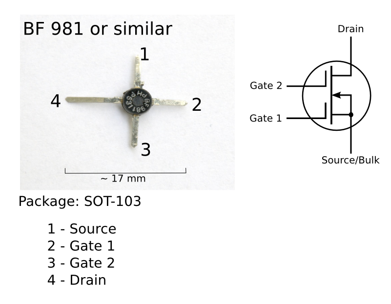 A multigate device, multi-gate MOSFET or multi-gate field-effect transistor (MuGFET) refers to a metal–oxide–semiconductor field-effect transistor (MOSFET) that has more than one
 Dozens of multigate transistor variants may be found in the literature. In general, these variants may be differentiated and classified in terms of architecture (planar vs. non-planar design) and the number of channels/gates (2, 3, or 4).

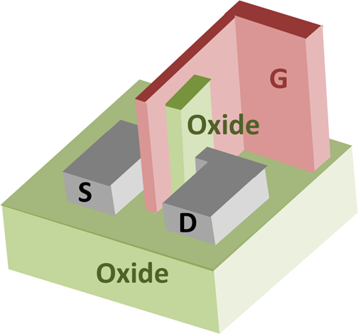
 FinFET (fin field-effect transistor) is a type of non-planar transistor, or "3D" transistor (not to be confused with 3D microchips). The FinFET is a variation on traditional MOSFETs distinguished by the presence of a thin silicon "fin" inversion channel on top of the substrate, allowing the gate to make two points of contact: the left and right sides of the fin. The thickness of the fin (measured in the direction from source to drain) determines the effective channel length of the device. The wrap-around gate structure provides a better electrical control over the channel and thus helps in reducing the leakage current and overcoming other
 BSIMCMG106.0.0, officially released on March 1, 2012 by UC Berkeley BSIM Group, is the first standard model for FinFETs. BSIM-CMG is implemented in Verilog-A. Physical surface-potential-based formulations are derived for both intrinsic and extrinsic models with finite body doping. The surface potentials at the source and drain ends are solved analytically with poly-depletion and quantum mechanical effects. The effect of finite body doping is captured through a perturbation approach. The analytic surface potential solution agrees closely with the 2-D device simulation results. If the channel doping concentration is low enough to be neglected, computational efficiency can be further improved by a setting a specific flag (COREMOD = 1).
All of the important multi-gate (MG) transistor behavior is captured by this model. Volume inversion is included in the solution of Poisson's equation, hence the subsequent I–V formulation automatically captures the volume-inversion effect. Analysis of electrostatic potential in the body of MG MOSFETs provided a model equation for short-channel effects (SCE). The extra electrostatic control from the end gates (top/bottom gates) (triple or quadruple-gate) is also captured in the short-channel model.
Inverted T-FET (Freescale Semiconductor)
Omega FinFET (TSMC)
Intel video explaining 3D ("Tri-Gate") chip and transistor design used in 22 nm architecture of Ivy Bridge
{{DEFAULTSORT:Multigate device MOSFETs Transistor types
 A multigate device, multi-gate MOSFET or multi-gate field-effect transistor (MuGFET) refers to a metal–oxide–semiconductor field-effect transistor (MOSFET) that has more than one
 gate
A gate or gateway is a point of entry to or from a space enclosed by walls. The word derived from old Norse "gat" meaning road or path; But other terms include ''yett and port''. The concept originally referred to the gap or hole in the wall ...
on a single transistor. The multiple gates may be controlled by a single gate electrode, wherein the multiple gate surfaces act electrically as a single gate, or by independent gate electrodes. A multigate device employing independent gate electrodes is sometimes called a multiple-independent-gate field-effect transistor (MIGFET). The most widely used multi-gate devices are the FinFET (fin field-effect transistor) and the GAAFET (gate-all-around field-effect transistor), which are non-planar transistors, or 3D transistors.
Multi-gate transistors are one of the several strategies being developed by MOS
MOS or Mos may refer to:
Technology
* MOSFET (metal–oxide–semiconductor field-effect transistor), also known as the MOS transistor
* Mathematical Optimization Society
* Model output statistics, a weather-forecasting technique
* MOS (filmm ...
semiconductor manufacturers to create ever-smaller microprocessors and memory cells, colloquially referred to as extending Moore's law
Moore's law is the observation that the number of transistors in a dense integrated circuit (IC) doubles about every two years. Moore's law is an observation and projection of a historical trend. Rather than a law of physics, it is an empir ...
(in its narrow, specific version concerning density scaling, exclusive of its careless historical conflation with Dennard scaling Dennard scaling, also known as MOSFET scaling, is a scaling law which states roughly that, as transistors get smaller, their power density stays constant, so that the power use stays in proportion with area; both voltage and current scale (downward) ...
). Development efforts into multigate transistors have been reported by the Electrotechnical Laboratory
The , or AIST, is a Japanese research facility headquartered in Tokyo, and most of the workforce is located in Tsukuba Science City, Ibaraki, and in several cities throughout Japan. The institute is managed to integrate scientific and engineeri ...
, Toshiba, Grenoble INP
The Grenoble Institute of Technology (Grenoble INP) (''Institut polytechnique de Grenoble'', ''Groupe Grenoble INP'' and before INPG) is a French technological university system consisting of eight engineering and management schools.
Grenoble INP ...
, Hitachi
() is a Japanese multinational corporation, multinational Conglomerate (company), conglomerate corporation headquartered in Chiyoda, Tokyo, Japan. It is the parent company of the Hitachi Group (''Hitachi Gurūpu'') and had formed part of the Ni ...
, IBM, TSMC, UC Berkeley, Infineon Technologies
Infineon Technologies AG is a German semiconductor manufacturer founded in 1999, when the semiconductor operations of the former parent company Siemens AG were spun off. Infineon has about 50,280 employees and is one of the ten largest semicond ...
, Intel, AMD, Samsung Electronics, KAIST, Freescale Semiconductor, and others, and the ITRS predicted correctly that such devices will be the cornerstone of sub-32 nm technologies. The primary roadblock to widespread implementation is manufacturability, as both planar and non-planar designs present significant challenges, especially with respect to lithography and patterning. Other complementary strategies for device scaling include channel strain engineering, silicon-on-insulator
In semiconductor manufacturing, silicon on insulator (SOI) technology is fabrication of silicon semiconductor devices in a layered silicon–insulator–silicon substrate, to reduce parasitic capacitance within the device, thereby improving perfo ...
-based technologies, and high-κ/metal gate materials.
Dual-gate MOSFETs are commonly used in very high frequency (VHF) mixers and in sensitive VHF front-end amplifiers. They are available from manufacturers such as Motorola, NXP Semiconductors
NXP Semiconductors N.V. (NXP) is a Dutch semiconductor designer and manufacturer with headquarters in Eindhoven, Netherlands. The company employs approximately 31,000 people in more than 30 countries. NXP reported revenue of $11.06 billion in 2 ...
, and Hitachi
() is a Japanese multinational corporation, multinational Conglomerate (company), conglomerate corporation headquartered in Chiyoda, Tokyo, Japan. It is the parent company of the Hitachi Group (''Hitachi Gurūpu'') and had formed part of the Ni ...
.
Types
 Dozens of multigate transistor variants may be found in the literature. In general, these variants may be differentiated and classified in terms of architecture (planar vs. non-planar design) and the number of channels/gates (2, 3, or 4).
Planar double-gate MOSFET (DGMOS)
A planar double-gate MOSFET (DGMOS) employs conventional planar (layer-by-layer) manufacturing processes to create double-gateMOSFET
The metal–oxide–semiconductor field-effect transistor (MOSFET, MOS-FET, or MOS FET) is a type of field-effect transistor (FET), most commonly fabricated by the controlled oxidation of silicon. It has an insulated gate, the voltage of which d ...
(metal–oxide–semiconductor field-effect transistor) devices, avoiding more stringent lithography requirements associated with non-planar, vertical transistor structures. In planar double-gate transistors the drain–source channel is sandwiched between two independently fabricated gate/gate-oxide stacks. The primary challenge in fabricating such structures is achieving satisfactory self-alignment between the upper and lower gates.
FlexFET
FlexFET is a planar, independently double-gated transistor with adamascene Damascene may refer to:
* Topics directly associated with the city of Damascus in Syria:
** A native or inhabitant of Damascus
** Damascus Arabic, the local dialect of Damascus
** Damascus steel, developed for swordmaking
** "Damascene moment", the ...
metal top gate MOSFET and an implanted JFET bottom gate that are self-aligned in a gate trench. This device is highly scalable due to its sub-lithographic channel length; non-implanted ultra-shallow source and drain extensions; non-epi raised source and drain regions; and gate-last flow. FlexFET is a true double-gate transistor in that (1) both the top and bottom gates provide transistor operation, and (2) the operation of the gates is coupled such that the top gate operation affects the bottom gate operation and vice versa. FlexFET was developed and is manufactured by American Semiconductor, Inc.
FinFET

 FinFET (fin field-effect transistor) is a type of non-planar transistor, or "3D" transistor (not to be confused with 3D microchips). The FinFET is a variation on traditional MOSFETs distinguished by the presence of a thin silicon "fin" inversion channel on top of the substrate, allowing the gate to make two points of contact: the left and right sides of the fin. The thickness of the fin (measured in the direction from source to drain) determines the effective channel length of the device. The wrap-around gate structure provides a better electrical control over the channel and thus helps in reducing the leakage current and overcoming other
 short-channel effect In electronics, short-channel effects occur in MOSFETs in which the channel length is comparable to the depletion layer widths of the source and drain junctions. These effects include, in particular, drain-induced barrier lowering, velocity saturati ...
s.
The first FinFET transistor type was called a "Depleted Lean-channel Transistor" or "DELTA" transistor, which was first fabricated by Hitachi Central Research Laboratory's Digh Hisamoto, Toru Kaga, Yoshifumi Kawamoto and Eiji Takeda in 1989. In the late 1990s, Digh Hisamoto began collaborating with an international team of researchers on further developing DELTA technology, including TSMC's Chenming Hu and a UC Berkeley research team including Tsu-Jae King Liu, Jeffrey Bokor, Xuejue Huang, Leland Chang, Nick Lindert, S. Ahmed, Cyrus Tabery, Yang-Kyu Choi, Pushkar Ranade, Sriram Balasubramanian, A. Agarwal and M. Ameen. In 1998, the team developed the first N-channel
The field-effect transistor (FET) is a type of transistor that uses an electric field to control the flow of current in a semiconductor. FETs (JFETs or MOSFETs) are devices with three terminals: ''source'', ''gate'', and ''drain''. FETs control ...
FinFETs and successfully fabricated devices down to a 17nm process. The following year, they developed the first P-channel
The field-effect transistor (FET) is a type of transistor that uses an electric field to control the flow of Electric current, current in a semiconductor. FETs (JFETs or MOSFETs) are devices with three terminals: ''source'', ''gate'', and ''dra ...
FinFETs. They coined the term "FinFET" (fin field-effect transistor) in a December 2000 paper.
In current usage the term FinFET has a less precise definition. Among microprocessor manufacturers, AMD, IBM, and Freescale describe their double-gate development efforts as FinFET development, whereas Intel avoids using the term when describing their closely related tri-gate architecture. In the technical literature, FinFET is used somewhat generically to describe any fin-based, multigate transistor architecture regardless of number of gates. It is common for a single FinFET transistor to contain several fins, arranged side by side and all covered by the same gate, that act electrically as one, to increase drive strength and performance. The gate may also cover the entirety of the fin(s).
A 25 nm transistor operating on just 0.7 volt was demonstrated in December 2002 by TSMC (Taiwan Semiconductor Manufacturing Company). The "Omega FinFET" design is named after the similarity between the Greek letter omega (Ω) and the shape in which the gate wraps around the source/drain structure. It has a gate delay of just 0.39 picosecond
A picosecond (abbreviated as ps) is a unit of time in the International System of Units (SI) equal to 10−12 or (one trillionth) of a second. That is one trillionth, or one millionth of one millionth of a second, or 0.000 000 000 ...
(ps) for the N-type transistor and 0.88 ps for the P-type.
In 2004, Samsung Electronics demonstrated a "Bulk FinFET" design, which made it possible to mass-produce FinFET devices. They demonstrated dynamic random-access memory (DRAM
Dynamic random-access memory (dynamic RAM or DRAM) is a type of random-access semiconductor memory that stores each bit of data in a memory cell, usually consisting of a tiny capacitor and a transistor, both typically based on metal-oxid ...
) manufactured with a 90nm
The 90 nm process refers to the level of MOSFET (CMOS) fabrication process technology that was commercialized by the 2003–2005 timeframe, by leading semiconductor companies like Toshiba, Sony, Samsung, IBM, Intel, Fujitsu, TSMC, Elpid ...
Bulk FinFET process. In 2006, a team of Korean researchers from the Korea Advanced Institute of Science and Technology
The Korea Advanced Institute of Science and Technology (KAIST) is a national research university located in Daedeok Innopolis, Daejeon, South Korea. KAIST was established by the Korean government in 1971 as the nation's first public, research ...
(KAIST) and the National Nano Fab Center developed a 3 nm transistor, the world's smallest nanoelectronic device, based on FinFET technology. In 2011, Rice University researchers Masoud Rostami and Kartik Mohanram demonstrated that FINFETs can have two electrically independent gates, which gives circuit designers more flexibility to design with efficient, low-power gates.
In 2012, Intel started using FinFETs for its future commercial devices. Leaks suggest that Intel's FinFET has an unusual shape of a triangle rather than rectangle, and it is speculated that this might be either because a triangle has a higher structural strength and can be more reliably manufactured or because a triangular prism has a higher area-to-volume ratio than a rectangular prism, thus increasing switching performance.
In September 2012, GlobalFoundries announced plans to offer a 14-nanometer process technology featuring FinFET three-dimensional transistors in 2014. The next month, the rival company TSMC announced start early or "risk" production of 16 nm FinFETs in November 2013.
In March 2014, TSMC announced that it is nearing implementation of several 16 nm
Sixteen or 16 may refer to:
*16 (number), the natural number following 15 and preceding 17
*one of the years 16 BC, AD 16, 1916, 2016
Films
* ''Pathinaaru'' or ''Sixteen'', a 2010 Tamil film
* Sixteen (1943 film), ''Sixteen'' (1943 film), a 194 ...
FinFETs die-on wafers manufacturing processes:
* 16 nm FinFET (Q4 2014),
* 16 nm FinFET+ ( Q4 2014),
* 16 nm FinFET "Turbo" (estimated in 2015–2016).
AMD released GPUs using their Polaris chip architecture and made on 14 nm FinFET in June 2016. The company has tried to produce a design to provide a "generational jump in power efficiency" while also offering stable frame rates for graphics, gaming, virtual reality, and multimedia applications.
In March 2017, Samsung and eSilicon
eSilicon was a fabless semiconductor company founded in 1999 in San Jose, California. eSilicon designs and manufactures digital CMOS and finFET ASICs. In addition, eSilicon designs market-specific semiconductor IP platforms and provides custom IC ...
announced the tapeout for production of a 14 nm FinFET ASIC in a 2.5D package.
Tri-gate transistor
A tri-gate transistor, also known as a triple-gate transistor, is a type of MOSFET with a gate on three of its sides. A triple-gate transistor was first demonstrated in 1987, by a Toshiba research team including K. Hieda, Fumio Horiguchi and H. Watanabe. They realized that the fully depleted (FD) body of a narrow bulk Si-based transistor helped improve switching due to a lessened body-bias effect. In 1992, a triple-gate MOSFET was demonstrated by IBM researcher Hon-Sum Wong. Intel announced this technology in September 2002. Intel announced "triple-gate transistors" which maximize "transistor switching performance and decreases power-wasting leakage". A year later, in September 2003, AMD announced that it was working on similar technology at the International Conference on Solid State Devices and Materials. No further announcements of this technology were made until Intel's announcement in May 2011, although it was stated at IDF 2011, that they demonstrated a working SRAM chip based on this technology at IDF 2009. On April 23, 2012, Intel released a new line of CPUs, termed Ivy Bridge, which feature tri-gate transistors. Intel has been working on its tri-gate architecture since 2002, but it took until 2011 to work out mass-production issues. The new style of transistor was described on May 4, 2011, in San Francisco. It was announced that Intel's factories were expected to make upgrades over 2011 and 2012 to be able to manufacture the Ivy Bridge CPUs. It was announced that the new transistors would also be used in Intel's Atom chips for low-powered devices. Tri-gate fabrication was used by Intel for the non-planar transistor architecture used in Ivy Bridge, Haswell andSkylake Skylake or Sky Lake may refer to:
* Skylake (microarchitecture), the codename for a processor microarchitecture developed by Intel as the successor to Broadwell
* Skylake (Mysia), a town of ancient Mysia, now in Turkey
* Sky Lake, Florida
Sky La ...
processors. These transistors employ a single gate stacked on top of two vertical gates (a single gate wrapped over three sides of the channel), allowing essentially three times the surface area for electrons to travel. Intel reports that their tri-gate transistors reduce leakage and consume far less power than previous transistors. This allows up to 37% higher speed or a power consumption at under 50% of the previous type of transistors used by Intel.
Intel explains: "The additional control enables as much transistor current flowing as possible when the transistor is in the 'on' state (for performance), and as close to zero as possible when it is in the 'off' state (to minimize power), and enables the transistor to switch very quickly between the two states (again, for performance)." Intel has stated that all products after Sandy Bridge will be based upon this design.
The term ''tri-gate'' is sometimes used generically to denote any multigate FET with three effective gates or channels.
Gate-all-around FET (GAAFET)
Gate-all-around FETs (GAAFETs) are the successor to FinFETs, as they can work at sizes below 7 nm. They were used by IBM to demonstrate 5 nm process technology. GAAFET, also known as a surrounding-gate transistor (SGT), is similar in concept to a FinFET except that the gate material surrounds the channel region on all sides. Depending on design, gate-all-around FETs can have two or four effective gates. Gate-all-around FETs have been successfully characterized both theoretically and experimentally. They have also been successfully etched onto nanowires of InGaAs, which have a higherelectron mobility
In solid-state physics, the electron mobility characterises how quickly an electron can move through a metal or semiconductor when pulled by an electric field. There is an analogous quantity for holes, called hole mobility. The term carrier mobili ...
than silicon.
A gate-all-around (GAA) MOSFET was first demonstrated in 1988, by a Toshiba research team including Fujio Masuoka
is a Japanese engineer, who has worked for Toshiba and Tohoku University, and is currently chief technical officer (CTO) of Unisantis Electronics. He is best known as the inventor of flash memory, including the development of both the NOR flash ...
, Hiroshi Takato, and Kazumasa Sunouchi, who demonstrated a vertical nanowire GAAFET which they called a "surrounding gate transistor" (SGT). Masuoka, best known as the inventor of flash memory
Flash memory is an electronic non-volatile computer memory storage medium that can be electrically erased and reprogrammed. The two main types of flash memory, NOR flash and NAND flash, are named for the NOR and NAND logic gates. Both us ...
, later left Toshiba and founded Unisantis Electronics in 2004 to research surrounding-gate technology along with Tohoku University. In 2006, a team of Korean researchers from the Korea Advanced Institute of Science and Technology
The Korea Advanced Institute of Science and Technology (KAIST) is a national research university located in Daedeok Innopolis, Daejeon, South Korea. KAIST was established by the Korean government in 1971 as the nation's first public, research ...
(KAIST) and the National Nano Fab Center developed a 3 nm transistor, the world's smallest nanoelectronic device, based on gate-all-around
A multigate device, multi-gate MOSFET or multi-gate field-effect transistor (MuGFET) refers to a metal–oxide–semiconductor field-effect transistor (MOSFET) that has more than one gate on a single transistor. The multiple gates may be control ...
(GAA) FinFET technology. GAAFET transistors may make use of high-k/metal gate materials. GAAFETs with up to 7 nanosheet A nanosheet is a two-dimensional nanostructure with thickness in a scale ranging from 1 to 100 nm.
A typical example of a nanosheet is graphene, the thinnest two-dimensional material (0.34 nm) in the world. It consists of a single layer o ...
s have been demonstrated which allow for improved performance and/or reduced device footprint. The widths of the nanosheets in GAAFETs is controllable which more easily allows for the adjustment of device characteristics.
As of 2020, Samsung and Intel have announced plans to mass produce GAAFET transistors (specifically MBCFET transistors) while TSMC has announced that they will continue to use FinFETs in their 3 nm node, despite TSMC developing GAAFET transistors.
Multi-bridge channel (MBC) FET
A multi-bridge channel FET (MBCFET) is similar to a GAAFET except for the use of nanosheets instead of nanowires. MBCFET is a word mark (trademark) registered in the U.S. to Samsung Electronics. Samsung plans on mass producing MBCFET transistors at the3 nm
In semiconductor manufacturing, the 3 nm process is the next die shrink after the 5 nanometer MOSFET (metal–oxide–semiconductor field-effect transistor) technology node. , Taiwanese chip manufacturer TSMC plans to put a 3 nm, semi ...
node for its foundry customers. Intel is also developing RibbonFET, a variation of MBCFET "nanoribbon" transistors. Unlike FinFETs, both the width and the number of the sheets can be varied to adjust drive strength or the amount of current the transistor can drive at a given voltage. The sheets often vary from 8 to 50 nanometers in width. The width of the nanosheets is known as Weff, or effective width.
Industry need
Planar transistors have been the core of integrated circuits for several decades, during which the size of the individual transistors has steadily decreased. As the size decreases, planar transistors increasingly suffer from the undesirable short-channel effect, especially "off-state" leakage current, which increases the idle power required by the device. In a multigate device, the channel is surrounded by several gates on multiple surfaces. Thus it provides better electrical control over the channel, allowing more effective suppression of "off-state" leakage current. Multiple gates also allow enhanced current in the "on" state, also known as drive current. Multigate transistors also provide a better analog performance due to a higher intrinsic gain and lower channel length modulation. These advantages translate to lower power consumption and enhanced device performance. Nonplanar devices are also more compact than conventional planar transistors, enabling higher transistor density which translates to smaller overall microelectronics.Integration challenges
The primary challenges to integrating nonplanar multigate devices into conventional semiconductor manufacturing processes include: * Fabrication of a thin silicon "fin" tens of nanometers wide * Fabrication of matched gates on multiple sides of the finCompact modeling
 BSIMCMG106.0.0, officially released on March 1, 2012 by UC Berkeley BSIM Group, is the first standard model for FinFETs. BSIM-CMG is implemented in Verilog-A. Physical surface-potential-based formulations are derived for both intrinsic and extrinsic models with finite body doping. The surface potentials at the source and drain ends are solved analytically with poly-depletion and quantum mechanical effects. The effect of finite body doping is captured through a perturbation approach. The analytic surface potential solution agrees closely with the 2-D device simulation results. If the channel doping concentration is low enough to be neglected, computational efficiency can be further improved by a setting a specific flag (COREMOD = 1).
All of the important multi-gate (MG) transistor behavior is captured by this model. Volume inversion is included in the solution of Poisson's equation, hence the subsequent I–V formulation automatically captures the volume-inversion effect. Analysis of electrostatic potential in the body of MG MOSFETs provided a model equation for short-channel effects (SCE). The extra electrostatic control from the end gates (top/bottom gates) (triple or quadruple-gate) is also captured in the short-channel model.
See also
* Three-dimensional integrated circuit *Semiconductor device
A semiconductor device is an electronic component that relies on the electronic properties of a semiconductor material (primarily silicon, germanium, and gallium arsenide, as well as organic semiconductors) for its function. Its conductivity li ...
* Clock gating
* High-κ dielectric
* Next-generation lithography
Next-generation lithography or NGL is a term used in integrated circuit manufacturing to describe the photolithography, lithography technologies in development which are intended to replace current techniques. The term applies to any lithography ...
* Extreme ultraviolet lithography
Extreme ultraviolet lithography (also known as EUV or EUVL) is an optical lithography technology used in steppers, machines that make integrated circuits (ICs) for computers and other electronic devices. It uses a range of extreme ultraviolet (EUV) ...
* Immersion lithography
Immersion lithography is a photolithography resolution enhancement technique for manufacturing integrated circuits (ICs) that replaces the usual air gap between the final lens and the wafer surface with a liquid medium that has a refractive inde ...
* Strain engineering
* Very Large Scale Integration (VLSI)
* Neuromorphic engineering
* Bit slicing
* 3D printing
3D printing or additive manufacturing is the Manufacturing, construction of a three-dimensional object from a computer-aided design, CAD model or a digital 3D modeling, 3D model. It can be done in a variety of processes in which material is ...
* Silicon on insulator
In semiconductor manufacturing, silicon on insulator (SOI) technology is fabrication of silicon semiconductor devices in a layered silicon–insulator–silicon substrate, to reduce parasitic capacitance within the device, thereby improving perfo ...
(SOI)
* MOSFET
The metal–oxide–semiconductor field-effect transistor (MOSFET, MOS-FET, or MOS FET) is a type of field-effect transistor (FET), most commonly fabricated by the controlled oxidation of silicon. It has an insulated gate, the voltage of which d ...
* Floating-gate MOSFET
* Transistor
* BSIM
* High-electron-mobility transistor
* Field-effect transistor
* JFET
The junction-gate field-effect transistor (JFET) is one of the simplest types of field-effect transistor. JFETs are three-terminal semiconductor devices that can be used as electronically controlled switches or resistors, or to build amplifiers. ...
* Tetrode transistor
* Pentode transistor A pentode transistor is any transistor having five active terminals.
Early pentode transistors
One early pentode transistor was developed in the early 1950s as an improvement over the point-contact transistor.
*A point-contact transistor having thr ...
* Memristor
* Quantum circuit
* Quantum logic gate
In quantum computing and specifically the quantum circuit model of computation, a quantum logic gate (or simply quantum gate) is a basic quantum circuit operating on a small number of qubits. They are the building blocks of quantum circuits, lik ...
* Transistor model
* Die shrink
References
External links
Inverted T-FET (Freescale Semiconductor)
Omega FinFET (TSMC)
Intel video explaining 3D ("Tri-Gate") chip and transistor design used in 22 nm architecture of Ivy Bridge
{{DEFAULTSORT:Multigate device MOSFETs Transistor types