|
Nanoelectronic
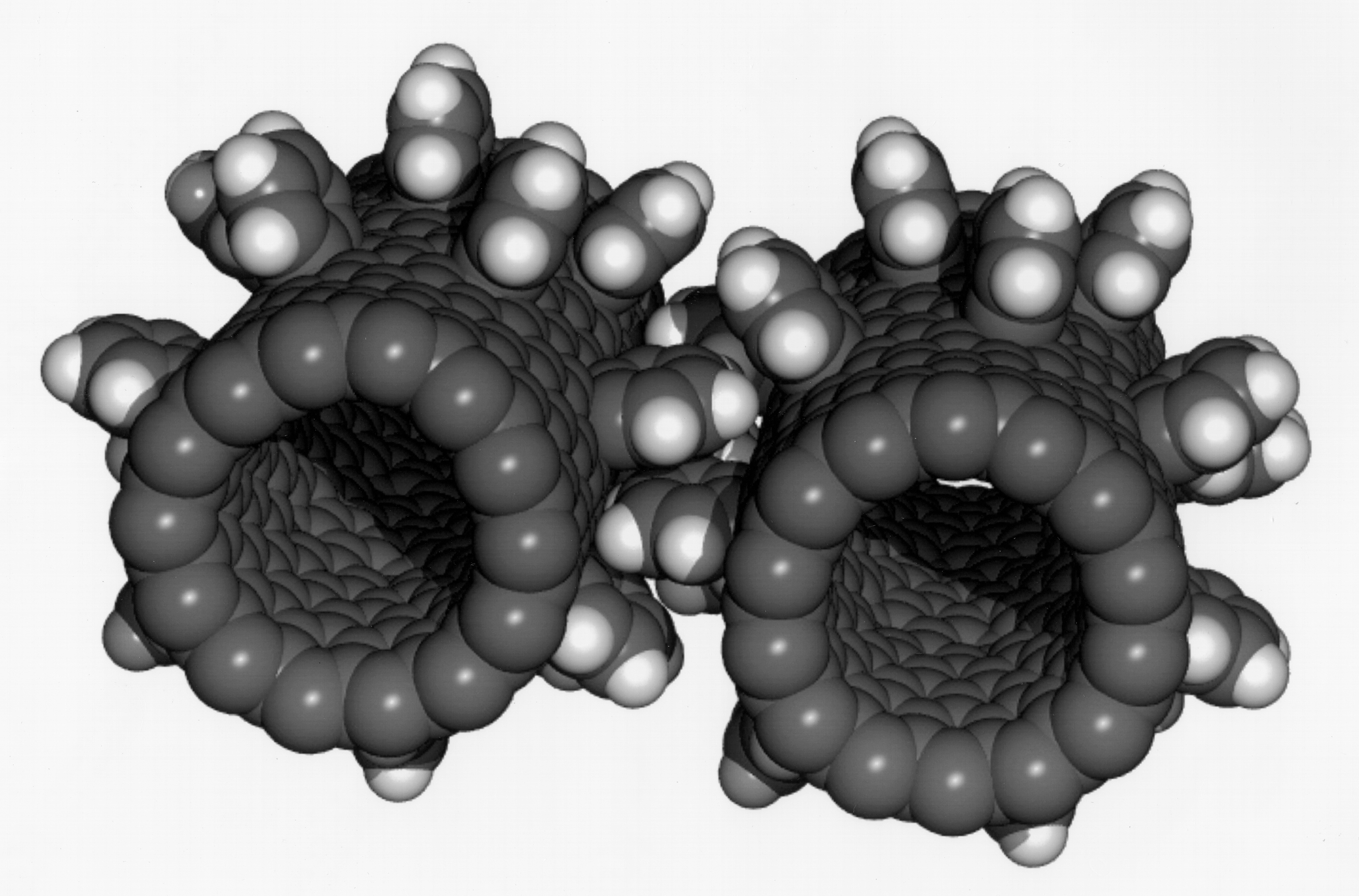
Nanoelectronics refers to the use of nanotechnology in electronic components. The term covers a diverse set of devices and materials, with the common characteristic that they are so small that inter-atomic interactions and quantum mechanical properties need to be studied extensively. Some of these candidates include: hybrid molecular/semiconductor electronics, one-dimensional nanotubes/nanowires (e.g. carbon nanotube or silicon nanowires) or advanced molecular electronics. Nanoelectronic devices have critical dimensions with a size range between 1 nm and 100 nm. Recent silicon MOSFET (metal–oxide–semiconductor field-effect transistor, or MOS transistor) technology generations are already within this regime, including 22 nanometers CMOS (complementary MOS) nodes and succeeding 14 nm, 10 nm and 7 nm FinFET (fin field-effect transistor) generations. Nanoelectronics is sometimes considered as disruptive technology because present candidates are significantly diffe ... [...More Info...] [...Related Items...] OR: [Wikipedia] [Google] [Baidu] |
Nanotechnology
Nanotechnology is the manipulation of matter with at least one dimension sized from 1 to 100 nanometers (nm). At this scale, commonly known as the nanoscale, surface area and quantum mechanical effects become important in describing properties of matter. This definition of nanotechnology includes all types of research and technologies that deal with these special properties. It is common to see the plural form "nanotechnologies" as well as "nanoscale technologies" to refer to research and applications whose common trait is scale. An earlier understanding of nanotechnology referred to the particular technological goal of precisely manipulating atoms and molecules for fabricating macroscale products, now referred to as molecular nanotechnology. Nanotechnology defined by scale includes fields of science such as surface science, organic chemistry, molecular biology, semiconductor physics, energy storage, engineering, microfabrication, and molecular engineering. The associated rese ... [...More Info...] [...Related Items...] OR: [Wikipedia] [Google] [Baidu] |
FinFET
A fin field-effect transistor (FinFET) is a multigate device, a MOSFET (metal–oxide–semiconductor field-effect transistor) built on a substrate where the gate is placed on two, three, or four sides of the channel or wrapped around the channel (gate all around), forming a double or even multi gate structure. These devices have been given the generic name "FinFETs" because the source/drain region forms fins on the silicon surface. The FinFET devices exhibit significantly faster switching times and higher current density than planar CMOS (complementary metal–oxide–semiconductor) technology, resulting in enhanced performance and power efficienc FinFET is a type of non-planar transistor, or "3D" transistor. It is the basis for modern nanoelectronic semiconductor device fabrication. Microchips utilizing FinFET gates first became commercialized in the first half of the 2010s, and became the dominant gate design at 14 nm, 10 nm and 7 nm process nodes. It is common for a ... [...More Info...] [...Related Items...] OR: [Wikipedia] [Google] [Baidu] |
Gordon Moore
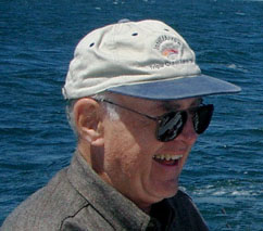
Gordon Earle Moore (January 3, 1929 – March 24, 2023) was an American businessman, engineer, and the co-founder and emeritus chairman of Intel Corporation. He proposed Moore's law which makes the observation that the number of transistors in an integrated circuit (IC) doubles about every two years. Early life and education Gordon Moore was born in 1929 as the second son of Walter Harold Moore (a sheriff in San Mateo County) and Florence Almira "Mira" Williamson (a homemaker). When Moore started school in 1935, the faculty noted his introverted personality. His father accepted a promotion to deputy sheriff in 1938 and moved the family to Redwood City, California. In 1940, Moore received a chemistry set as a Christmas gift, which inspired him to become a chemist. From 1942 to 1946, Moore studied at Sequoia High School, where he was involved in athletic activities. From 1946 to 1947, Moore attended San José State College (now San José State University), studying chemistry. ... [...More Info...] [...Related Items...] OR: [Wikipedia] [Google] [Baidu] |
Silicon Nanowire
Silicon nanowires, also referred to as SiNWs, are a type of semiconductor nanowire most often formed from a silicon precursor by etching of a solid or through catalyzed growth from a vapor or liquid phase. Such nanowires have promising applications in lithium-ion batteries, thermoelectrics and sensors. Initial synthesis of SiNWs is often accompanied by thermal oxidation steps to yield structures of accurately tailored size and morphology. SiNWs have unique properties that are not seen in bulk (three-dimensional) silicon materials. These properties arise from an unusual quasi one-dimensional electronic structure and are the subject of research across numerous disciplines and applications. The reason that SiNWs are considered one of the most important one-dimensional materials is they could have a function as building blocks for nanoscale electronics assembled without the need for complex and costly fabrication facilities. SiNWs are frequently studied towards applications including ph ... [...More Info...] [...Related Items...] OR: [Wikipedia] [Google] [Baidu] |
3 Nanometer
In semiconductor manufacturing, the 3 nm process is the next die shrink after the 5 nm MOSFET (metal–oxide–semiconductor field-effect transistor) technology node. South Korean chipmaker Samsung started shipping its 3 nm gate all around (GAA) process, named 3GAA, in mid-2022. On 29 December 2022, Taiwanese chip manufacturer TSMC announced that volume production using its 3 nm semiconductor node (N3) was underway with good yields. An enhanced 3 nm chip process called "N3E" may have started production in 2023. American manufacturer Intel planned to start 3 nm production in 2023. Samsung's 3 nm process is based on GAAFET (gate-all-around field-effect transistor) technology, a type of multi-gate MOSFET technology, while TSMC's 3 nm process still uses FinFET (fin field-effect transistor) technology, despite TSMC developing GAAFET transistors. Specifically, Samsung plans to use its own variant of GAAFET called MBCFET (multi-bridge channel field ... [...More Info...] [...Related Items...] OR: [Wikipedia] [Google] [Baidu] |
Moore's Law
Moore's law is the observation that the Transistor count, number of transistors in an integrated circuit (IC) doubles about every two years. Moore's law is an observation and Forecasting, projection of a historical trend. Rather than a law of physics, it is an empirical relationship. It is an experience-curve law, a type of law quantifying efficiency gains from experience in production. The observation is named after Gordon Moore, the co-founder of Fairchild Semiconductor and Intel and former CEO of the latter, who in 1965 noted that the number of components per integrated circuit had been exponential growth, doubling every year, and projected this rate of growth would continue for at least another decade. In 1975, looking forward to the next decade, he revised the forecast to doubling every two years, a compound annual growth rate (CAGR) of 41%. Moore's empirical evidence did not directly imply that the historical trend would continue, nevertheless, his prediction has held si ... [...More Info...] [...Related Items...] OR: [Wikipedia] [Google] [Baidu] |
CMOS
Complementary metal–oxide–semiconductor (CMOS, pronounced "sea-moss ", , ) is a type of MOSFET, metal–oxide–semiconductor field-effect transistor (MOSFET) semiconductor device fabrication, fabrication process that uses complementary and symmetrical pairs of p-type semiconductor, p-type and n-type semiconductor, n-type MOSFETs for logic functions. CMOS technology is used for constructing integrated circuit (IC) chips, including microprocessors, microcontrollers, memory chips (including Nonvolatile BIOS memory, CMOS BIOS), and other digital logic circuits. CMOS technology is also used for analog circuits such as image sensors (CMOS sensors), data conversion, data converters, RF circuits (RF CMOS), and highly integrated transceivers for many types of communication. In 1948, Bardeen and Brattain patented an insulated-gate transistor (IGFET) with an inversion layer. Bardeen's concept forms the basis of CMOS technology today. The CMOS process was presented by Fairchild Semico ... [...More Info...] [...Related Items...] OR: [Wikipedia] [Google] [Baidu] |
Friction
Friction is the force resisting the relative motion of solid surfaces, fluid layers, and material elements sliding against each other. Types of friction include dry, fluid, lubricated, skin, and internal -- an incomplete list. The study of the processes involved is called tribology, and has a history of more than 2000 years. Friction can have dramatic consequences, as illustrated by the use of friction created by rubbing pieces of wood together to start a fire. Another important consequence of many types of friction can be wear, which may lead to performance degradation or damage to components. It is known that frictional energy losses account for about 20% of the total energy expenditure of the world. As briefly discussed later, there are many different contributors to the retarding force in friction, ranging from asperity deformation to the generation of charges and changes in local structure. When two bodies in contact move relative to each other, due to these variou ... [...More Info...] [...Related Items...] OR: [Wikipedia] [Google] [Baidu] |
Drill
A drill is a tool used for making round holes or driving fasteners. It is fitted with a drill bit for making holes, or a screwdriver bit for securing fasteners. Historically, they were powered by hand, and later mains power, but cordless battery-powered drills are proliferating due to increased efficiency and ease of use. Drills are commonly used in woodworking, metalworking, construction, machine tool fabrication, and utility projects. Specially designed versions are made for surgery, dentistry, miniatures, and other applications. History Around 35,000 BC, ''Homo sapiens'' discovered the benefits of the application of rotary tools. This would have rudimentarily consisted of a pointed rock being spun between the hands to bore a hole through another material. This led to the hand drill, a smooth stick, that was sometimes attached to flint point, and was rubbed between the palms. This was used by many ancient civilizations around the world including the Mayans. The ear ... [...More Info...] [...Related Items...] OR: [Wikipedia] [Google] [Baidu] |
Power (physics)
Power is the amount of energy transferred or converted per unit time. In the International System of Units, the unit of power is the watt, equal to one joule per second. Power is a Scalar (physics), scalar quantity. Specifying power in particular systems may require attention to other quantities; for example, the power involved in moving a ground vehicle is the product of the aerodynamic drag plus traction (engineering), traction force on the wheels, and the velocity of the vehicle. The output power of a Engine, motor is the product of the torque that the motor generates and the angular velocity of its output shaft. Likewise, the power dissipated in an electrical element of a electrical circuit, circuit is the product of the electric current, current flowing through the element and of the voltage across the element. Definition Power is the Rate (mathematics), rate with respect to time at which work is done or, more generally, the rate of change of total mechanical energy. It is ... [...More Info...] [...Related Items...] OR: [Wikipedia] [Google] [Baidu] |
Surface Area
The surface area (symbol ''A'') of a solid object is a measure of the total area that the surface of the object occupies. The mathematical definition of surface area in the presence of curved surfaces is considerably more involved than the definition of arc length of one-dimensional curves, or of the surface area for polyhedra (i.e., objects with flat polygonal faces), for which the surface area is the sum of the areas of its faces. Smooth surfaces, such as a sphere, are assigned surface area using their representation as parametric surfaces. This definition of surface area is based on methods of infinitesimal calculus and involves partial derivatives and double integration. A general definition of surface area was sought by Henri Lebesgue and Hermann Minkowski at the turn of the twentieth century. Their work led to the development of geometric measure theory, which studies various notions of surface area for irregular objects of any dimension. An important example is ... [...More Info...] [...Related Items...] OR: [Wikipedia] [Google] [Baidu] |


