Poly Depletion on:
[Wikipedia]
[Google]
[Amazon]
Polysilicon depletion effect is the phenomenon in which unwanted variation of
 ''Vgs'' = Gate Voltage
''Vth'' = Threshold Voltage
n+ = Highly doped N region In ''figure 1(a) of'' an '' nMOS'' transistor it is observed that the free majority carriers are scattered throughout the structure because of the absence of an external In an NMOS with n+ Polysilicon gate, the poly depletion effect aids in the channel formation by the combined effect of the ''(+)ve'' field of donor ions (ND) and the externally applied ''(+)ve'' field at gate terminal. Basically the accumulation of the ''(+)ve'' charged Donor
Reduction of Polysilicon Gate Depletion Effect in NMOS
*
Fabrication of microprocessor by intel
threshold voltage
The threshold voltage, commonly abbreviated as Vth or VGS(th), of a field-effect transistor (FET) is the minimum gate-to-source voltage (VGS) that is needed to create a conducting path between the source and drain terminals. It is an important s ...
of the MOSFET
upright=1.3, Two power MOSFETs in amperes">A in the ''on'' state, dissipating up to about 100 watt">W and controlling a load of over 2000 W. A matchstick is pictured for scale.
In electronics, the metal–oxide–semiconductor field- ...
devices using polysilicon
Polycrystalline silicon, or multicrystalline silicon, also called polysilicon, poly-Si, or mc-Si, is a high purity, polycrystalline form of silicon, used as a raw material by the solar photovoltaic and electronics industry.
Polysilicon is produ ...
as gate material is observed, leading to unpredicted behavior of the electronic circuit
An electronic circuit is composed of individual electronic components, such as resistors, transistors, capacitors, inductors and diodes, connected by conductive wires or Conductive trace, traces through which electric current can flow. It is a t ...
. Because of this variation High-k Dielectric Metal Gates (HKMG) were introduced to solve the issue.
Polycrystalline silicon
Polycrystalline silicon, or multicrystalline silicon, also called polysilicon, poly-Si, or mc-Si, is a high purity, polycrystalline form of silicon, used as a raw material by the solar photovoltaic and electronics industry.
Polysilicon is produc ...
, also called polysilicon, is a material consisting of small silicon crystals. The latter differs from monocrystalline silicon
Monocrystalline silicon, often referred to as single-crystal silicon or simply mono-Si, is a critical material widely used in modern electronics and photovoltaics. As the foundation for silicon-based discrete components and integrated circuits, ...
used for semiconductor electronics
A semiconductor device is an electronic component that relies on the electronic properties of a semiconductor material (primarily silicon, germanium, and gallium arsenide, as well as organic semiconductors) for its function. Its conductivity l ...
and solar cells
A solar cell, also known as a photovoltaic cell (PV cell), is an electronic device that converts the energy of light directly into electricity by means of the photovoltaic effect.
, and from amorphous silicon
Amorphous silicon (a-Si) is the non-crystalline form of silicon used for solar cells and thin-film transistors in LCDs.
Used as semiconductor material for a-Si solar cells, or thin-film silicon solar cells, it is deposited in thin films onto ...
, used for thin film devices and solar cells.
Gate material choice
The gate contact may be ofpolysilicon
Polycrystalline silicon, or multicrystalline silicon, also called polysilicon, poly-Si, or mc-Si, is a high purity, polycrystalline form of silicon, used as a raw material by the solar photovoltaic and electronics industry.
Polysilicon is produ ...
or metal, previously polysilicon was chosen over metal because the interfacing between polysilicon and gate oxide
The gate oxide is the dielectric layer that separates the metal gate, gate terminal of a MOSFET (metal–oxide–semiconductor field-effect transistor) from the underlying source and drain terminals as well as the conductive channel that connects ...
( SiO2) was favorable. But the conductivity of the poly-silicon layer is very low and because of this low conductivity, the charge accumulation is low, leading to a delay in channel formation and thus unwanted delays in circuits. The poly layer is doped with N-type or P-type impurity to make it behave like a perfect conductor and reduce the delay.
Doped polysilicon gate disadvantages
 ''Vgs'' = Gate Voltage
''Vth'' = Threshold Voltage
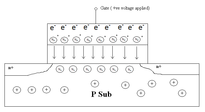
n+ = Highly doped N region In ''figure 1(a) of'' an '' nMOS'' transistor it is observed that the free majority carriers are scattered throughout the structure because of the absence of an external
electric field
An electric field (sometimes called E-field) is a field (physics), physical field that surrounds electrically charged particles such as electrons. In classical electromagnetism, the electric field of a single charge (or group of charges) descri ...
. When a positive field is applied on the gate, the scattered carriers arrange themselves like ''figure 1(b)'', the electrons move closer toward the gate terminal but due to the open circuit configuration they don't start to flow. As a result of the separation of charges a depletion region is formed on the polysilicon-oxide interface, which has a direct effect on the channel formation in MOSFET
upright=1.3, Two power MOSFETs in amperes">A in the ''on'' state, dissipating up to about 100 watt">W and controlling a load of over 2000 W. A matchstick is pictured for scale.
In electronics, the metal–oxide–semiconductor field- ...
s.
 In an NMOS with n+ Polysilicon gate, the poly depletion effect aids in the channel formation by the combined effect of the ''(+)ve'' field of donor ions (ND) and the externally applied ''(+)ve'' field at gate terminal. Basically the accumulation of the ''(+)ve'' charged Donor
 ions
An ion () is an atom or molecule with a net electrical charge. The charge of an electron is considered to be negative by convention and this charge is equal and opposite to the charge of a proton, which is considered to be positive by convent ...
(ND) on the polysilicon enhances the Formation of the inversion channel and when ' an inversion layer is formed, which can be seen in the figure 1(b) where the inversion channel is formed of acceptor ions (NA) ( minority carriers). Polysilicon depletion can vary laterally across a transistor depending on the fabrication process, which can lead to significant transistor variability in certain transistor dimensions.
Metal gates re-introduced
For the above reason as the devices go down on the scaling (32-28nm nodes) poly gates are being replaced by metal gates. The following technology is known as High-k Dielectric Metal Gate (HKMG) integration. In 2011Intel
Intel Corporation is an American multinational corporation and technology company headquartered in Santa Clara, California, and Delaware General Corporation Law, incorporated in Delaware. Intel designs, manufactures, and sells computer compo ...
has released a press-kit regarding their fabrication procedures of different nodes, which showed the use of Metal gate technology.
Doped polysilicon was preferred earlier as gate material in MOS devices. Polysilicons were used as their work function
In solid-state physics, the work function (sometimes spelled workfunction) is the minimum thermodynamic work (i.e., energy) needed to remove an electron from a solid to a point in the vacuum immediately outside the solid surface. Here "immediately" ...
matched with the Si substrate (which results in the low threshold voltage
The threshold voltage, commonly abbreviated as Vth or VGS(th), of a field-effect transistor (FET) is the minimum gate-to-source voltage (VGS) that is needed to create a conducting path between the source and drain terminals. It is an important s ...
of MOSFET
upright=1.3, Two power MOSFETs in amperes">A in the ''on'' state, dissipating up to about 100 watt">W and controlling a load of over 2000 W. A matchstick is pictured for scale.
In electronics, the metal–oxide–semiconductor field- ...
). Metal gates were re-introduced at the time when SiO2 dielectric
In electromagnetism, a dielectric (or dielectric medium) is an Insulator (electricity), electrical insulator that can be Polarisability, polarised by an applied electric field. When a dielectric material is placed in an electric field, electric ...
s are being replaced by high-k dielectrics like Hafnium oxide
Hafnium(IV) oxide is the inorganic compound with the formula . Also known as hafnium dioxide or hafnia, this colourless solid is one of the most common and stable compounds of hafnium. It is an electrical insulator with a band gap of 5.3~5.7 eV. H ...
as gate oxide in the mainstream CMOS
Complementary metal–oxide–semiconductor (CMOS, pronounced "sea-moss
", , ) is a type of MOSFET, metal–oxide–semiconductor field-effect transistor (MOSFET) semiconductor device fabrication, fabrication process that uses complementary an ...
technology. Also at the interface with gate dielectric, Polysilicon forms an SiOx layer. Moreover, there remains a high probability for Fermi level pinning
Enrico Fermi (; 29 September 1901 – 28 November 1954) was an Italian and naturalized American physicist, renowned for being the creator of the world's first artificial nuclear reactor, the Chicago Pile-1, and a member of the Manhattan Project ...
to occur. So the effect with doped poly is an undesired reduction of threshold voltage that wasn't taken into account during circuit simulation. In order to avoid this kind of variation in vth of the MOSFET
upright=1.3, Two power MOSFETs in amperes">A in the ''on'' state, dissipating up to about 100 watt">W and controlling a load of over 2000 W. A matchstick is pictured for scale.
In electronics, the metal–oxide–semiconductor field- ...
, at present metal gate is preferred over Polysilicon
Polycrystalline silicon, or multicrystalline silicon, also called polysilicon, poly-Si, or mc-Si, is a high purity, polycrystalline form of silicon, used as a raw material by the solar photovoltaic and electronics industry.
Polysilicon is produ ...
.
See also
Reduction of Polysilicon Gate Depletion Effect in NMOS
*
Drain-induced barrier lowering
Drain-induced barrier lowering (DIBL) is a short-channel effect in MOSFETs referring originally to a reduction of threshold voltage of the transistor at higher drain voltages.
In a classic planar field-effect transistor with a long channel, the b ...
* Gate materialFabrication of microprocessor by intel
References
{{Reflist Transistors Semiconductor devices Semiconductor technology MOSFETs