|
Celsius (microarchitecture)
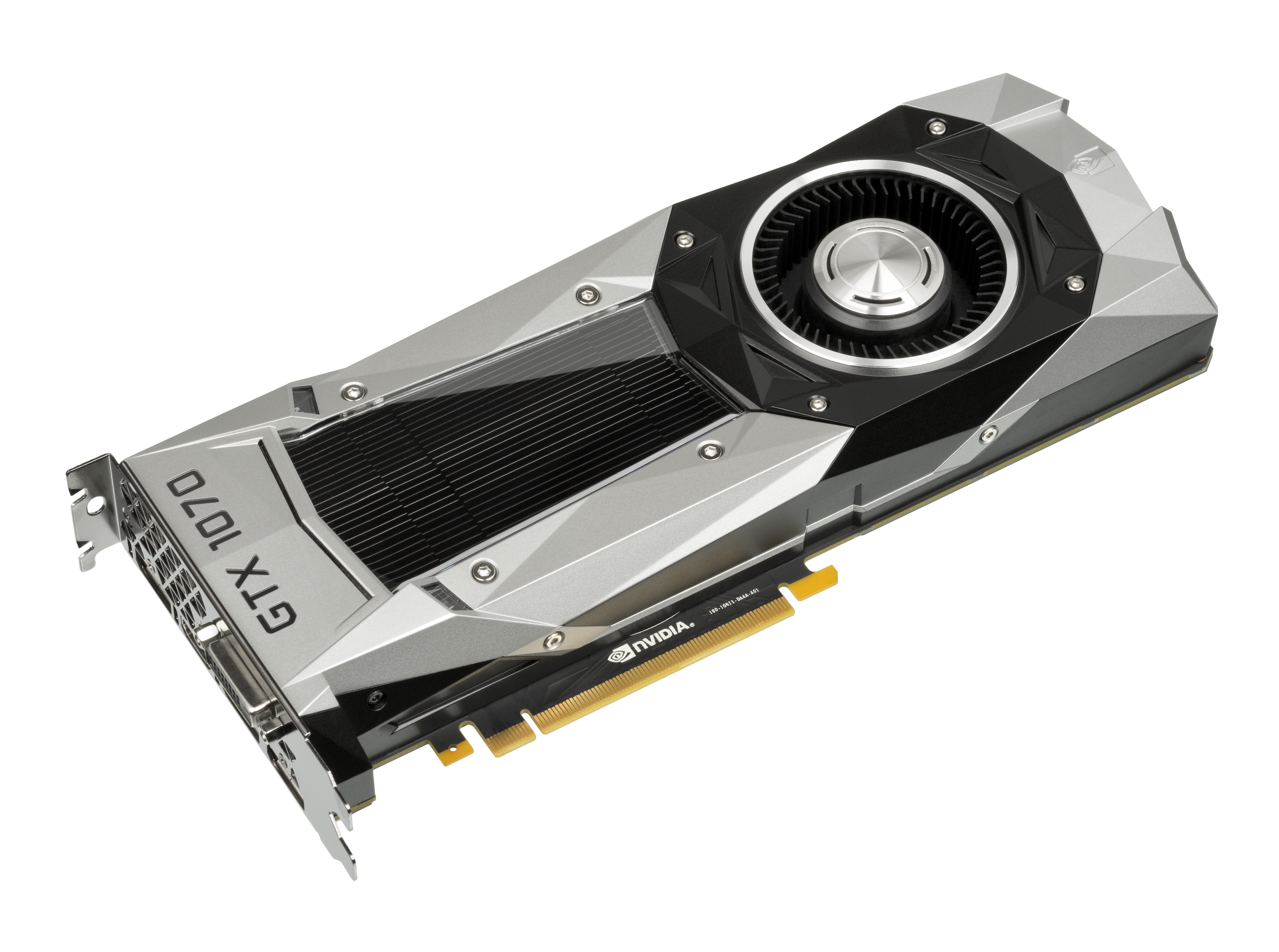
Celsius is the codename for a GPU microarchitecture developed by Nvidia, and released in 1999, as the successor to Fahrenheit (NV4, NV3...) microarchitecture. It was named with reference to Celsius and used with the GeForce 256 and GeForce 2 series. Graphics features * DirectX 7.0 * OpenGL 1.2 (1.5) * Max VRAM size bumped to 128MB Chips GeForce 256 * NV10, 17 million transistor GeForce 2 series * NV11, 20 million transistor * NV15, 25 million transistor * NV17, 29 million transistor * NV18, 29 million transistor * Crush11, 20 million transistor * Crush17, 29 million transistor GPU list GeForce 256 GeForce 2 series See also * List of Nvidia graphics processing units * Scalable Link Interface (SLI) * Qualcomm Adreno Adreno is a series of graphics processing unit (GPU) semiconductor intellectual property cores developed by Qualcomm and used in many of their SoCs. History Adreno (an anagram of AMD's graphic card brand ''Radeon''), was originally d ... [...More Info...] [...Related Items...] OR: [Wikipedia] [Google] [Baidu] |
Fahrenheit (microarchitecture)
Fahrenheit is the codename for a GPU microarchitecture developed by Nvidia, and released in 1998, as the successor to STG-2000, Riva 128 (NV1, NV2, NV3...) microarchitecture. It was named with reference to Fahrenheit and used with STG-2000, Riva 128. Graphics features * DirectX 5.0 and 6.0 * OpenGL 1.2 *Vertex shader: None *Pixel shader: ? *Z-buffer 24 bits *Up to 2048*2048 pixels texture size *32-bit ( truecolor) pixel format (add since Riva TNT) * AGP 4X support *Bump Mapping in single cycle *Up to 32MB video memory GPU list See also * List of Nvidia graphics processing units * Scalable Link Interface (SLI) * Qualcomm Adreno * Celsius (microarchitecture) Celsius is the codename for a GPU microarchitecture developed by Nvidia, and released in 1999, as the successor to Fahrenheit (NV4, NV3...) microarchitecture. It was named with reference to Celsius and used with the GeForce 256 and GeForce 2 ser ... References {{Graphics Processing Unit GPGPU Nvid ... [...More Info...] [...Related Items...] OR: [Wikipedia] [Google] [Baidu] |
Megabyte
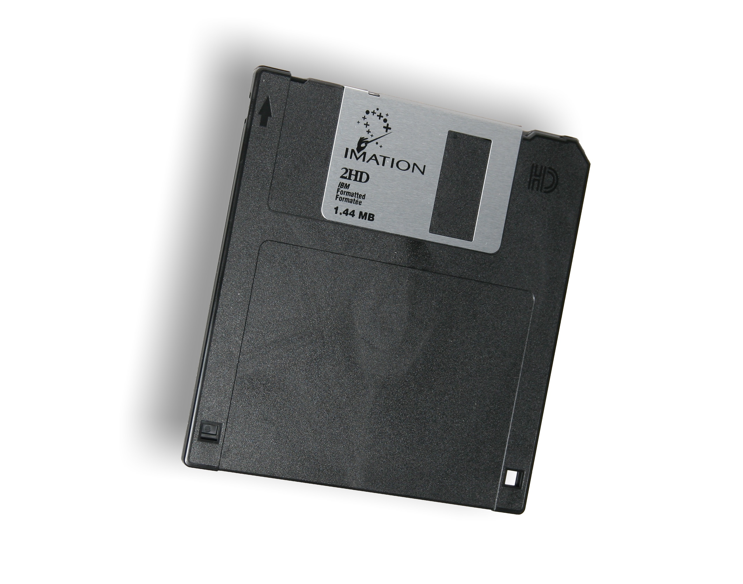
The megabyte is a multiple of the unit byte for digital information. Its recommended unit symbol is MB. The unit prefix ''mega'' is a multiplier of (106) in the International System of Units (SI). Therefore, one megabyte is one million bytes of information. This definition has been incorporated into the International System of Quantities. In the computer and information technology fields, other definitions have been used that arose for historical reasons of convenience. A common usage has been to designate one megabyte as (220 B), a quantity that conveniently expresses the binary architecture of digital computer memory. The standards bodies have deprecated this usage of the megabyte in favor of a new set of binary prefixes, in which this quantity is designated by the unit mebibyte (MiB). Definitions The unit megabyte is commonly used for 10002 (one million) bytes or 10242 bytes. The interpretation of using base 1024 originated as technical jargon for the byte multiples that ... [...More Info...] [...Related Items...] OR: [Wikipedia] [Google] [Baidu] |
Nvidia Microarchitectures
Nvidia CorporationOfficially written as NVIDIA and stylized in its logo as VIDIA with the lowercase "n" the same height as the uppercase "VIDIA"; formerly stylized as VIDIA with a large italicized lowercase "n" on products from the mid 1990s to early-mid 2000s. Though unofficial, second letter capitalization of NVIDIA, i.e. nVidia, may be found within enthusiast communities and publications. ( ) is an American multinational technology company incorporated in Delaware and based in Santa Clara, California. It is a software and fabless company which designs graphics processing units (GPUs), application programming interface (APIs) for data science and high-performance computing as well as system on a chip units (SoCs) for the mobile computing and automotive market. Nvidia is a global leader in artificial intelligence hardware and software. Its professional line of GPUs are used in workstations for applications in such fields as architecture, engineering and construction, media a ... [...More Info...] [...Related Items...] OR: [Wikipedia] [Google] [Baidu] |
Graphics Microarchitectures
Graphics () are visual images or designs on some surface, such as a wall, canvas, screen, paper, or stone, to inform, illustrate, or entertain. In contemporary usage, it includes a pictorial representation of data, as in design and manufacture, in typesetting and the graphic arts, and in educational and recreational software. Images that are generated by a computer are called computer graphics. Examples are photographs, drawings, line art, mathematical graphs, line graphs, charts, diagrams, typography, numbers, symbols, geometric designs, maps, engineering drawings, or other images. Graphics often combine text, illustration, and color. Graphic design may consist of the deliberate selection, creation, or arrangement of typography alone, as in a brochure, flyer, poster, web site, or book without any other element. The objective can be clarity or effective communication, association with other cultural elements, or merely the creation of a distinctive style. Graphics can be ... [...More Info...] [...Related Items...] OR: [Wikipedia] [Google] [Baidu] |
GPGPU
General-purpose computing on graphics processing units (GPGPU, or less often GPGP) is the use of a graphics processing unit (GPU), which typically handles computation only for computer graphics, to perform computation in applications traditionally handled by the central processing unit (CPU). The use of multiple video cards in one computer, or large numbers of graphics chips, further parallelizes the already parallel nature of graphics processing. Essentially, a GPGPU pipeline is a kind of parallel processing between one or more GPUs and CPUs that analyzes data as if it were in image or other graphic form. While GPUs operate at lower frequencies, they typically have many times the number of cores. Thus, GPUs can process far more pictures and graphical data per second than a traditional CPU. Migrating data into graphical form and then using the GPU to scan and analyze it can create a large speedup. GPGPU pipelines were developed at the beginning of the 21st century for grap ... [...More Info...] [...Related Items...] OR: [Wikipedia] [Google] [Baidu] |
Adreno
Adreno is a series of graphics processing unit (GPU) semiconductor intellectual property cores developed by Qualcomm and used in many of their SoCs. History Adreno (an anagram of AMD's graphic card brand ''Radeon''), was originally developed by ATI Technologies and sold to Qualcomm in 2009 for $65M, and was used in their mobile chipset products. Early Adreno models included the Adreno 100 and 110, which had 2D graphics acceleration and limited multimedia capabilities. At the time, 3D graphics on mobile platforms were commonly handled using software-based rendering engines, which limited their performance. With growing demand for more advanced multimedia and 3D graphics capabilities, Qualcomm licensed the Imageon IP from AMD, in order to add hardware-accelerated 3D capabilities to their mobile products. Further collaboration with AMD resulted in the development of the Adreno 200, originally named the AMD Z430, based on the R400 architecture used in the Xenos GPU of the Xbox ... [...More Info...] [...Related Items...] OR: [Wikipedia] [Google] [Baidu] |
Scalable Link Interface
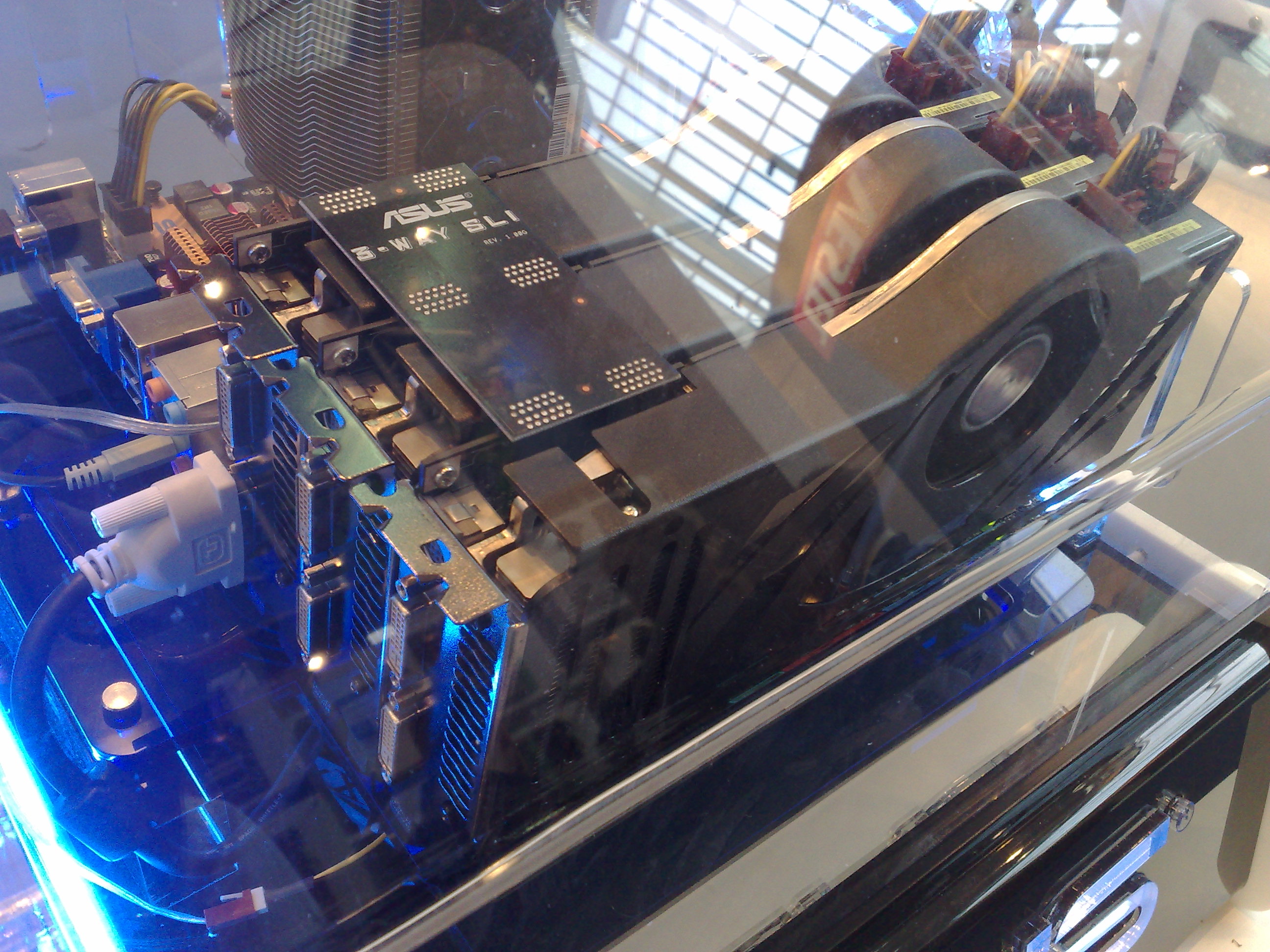
Scalable Link Interface (SLI) is a brand name for a deprecated multi- GPU technology developed by Nvidia for linking two or more video cards together to produce a single output. SLI is a parallel processing algorithm for computer graphics, meant to increase the available processing power. The initialism SLI was first used by 3dfx for Scan-Line Interleave, which was introduced to the consumer market in 1998 and used in the Voodoo2 line of video cards. After buying out 3dfx, Nvidia acquired the technology but did not use it. Nvidia later reintroduced the SLI name in 2004 and intended for it to be used in modern computer systems based on the PCI Express (PCIe) bus; however, the technology behind the name SLI has changed dramatically requirincompatible motherboards Implementation SLI allows two, three, or four graphics processing units (GPUs) to share the workload when rendering real-time 3D computer graphics. Ideally, identical GPUs are installed on the motherboard that con ... [...More Info...] [...Related Items...] OR: [Wikipedia] [Google] [Baidu] |
List Of Nvidia Graphics Processing Units
This list contains general information about graphics processing units (GPUs) and video cards from Nvidia, based on official specifications. In addition some Nvidia motherboards come with integrated onboard GPUs. Limited/Special/Collectors' Editions or AIB versions are not included. Field explanations The fields in the table listed below describe the following: * ''Model'' – The marketing name for the processor, assigned by The Nvidia. * ''Launch'' – Date of release for the processor. * ''Code name'' – The internal engineering codename for the processor (typically designated by an NVXY name and later GXY where X is the series number and Y is the schedule of the project for that generation). * ''Fab'' – Fabrication process. Average feature size of components of the processor. * ''Bus interface'' – Bus by which the graphics processor is attached to the system (typically an expansion slot, such as PCI, AGP, or PCI-Express). * ''Memory'' – The amount of graphics memory a ... [...More Info...] [...Related Items...] OR: [Wikipedia] [Google] [Baidu] |
180 Nm
The 180 nm process refers to the level of MOSFET ( CMOS) semiconductor process technology that was commercialized around the 1998–2000 timeframe by leading semiconductor companies, starting with TSMC and Fujitsu, then followed by Sony, Toshiba, Intel, AMD, Texas Instruments and IBM. The origin of the 180 nm value is historical, as it reflects a trend of 70% scaling every 2–3 years. The naming is formally determined by the International Technology Roadmap for Semiconductors (ITRS). Some of the first CPUs manufactured with this process include Intel Coppermine family of Pentium III processors. This was the first technology using a gate length shorter than that of light used for contemporary lithography, which had a wavelength of 193 nm. Some more recent microprocessors and microcontrollers (e.g. PIC) are using this technology because it is typically low cost and does not require upgrading of existing equipment. In 2022, Google sponsored open-source hardware p ... [...More Info...] [...Related Items...] OR: [Wikipedia] [Google] [Baidu] |
Double Data Rate
In computing, a computer bus operating with double data rate (DDR) transfers data on both the rising and falling edges of the clock signal. This is also known as double pumped, dual-pumped, and double transition. The term toggle mode is used in the context of NAND flash memory. Overview The simplest way to design a clocked electronic circuit is to make it perform one transfer per full cycle (rise and fall) of a clock signal. This, however, requires that the clock signal changes twice per transfer, while the data lines change at most once per transfer. When operating at a high bandwidth, signal integrity limitations constrain the clock frequency. By using both edges of the clock, the data signals operate with the same limiting frequency, thereby doubling the data transmission rate. This technique has been used for microprocessor front-side busses, Ultra-3 SCSI, expansion buses (AGP, PCI-X), graphics memory ( GDDR), main memory (both RDRAM and DDR1 through DDR5), and t ... [...More Info...] [...Related Items...] OR: [Wikipedia] [Google] [Baidu] |
SDR SDRAM
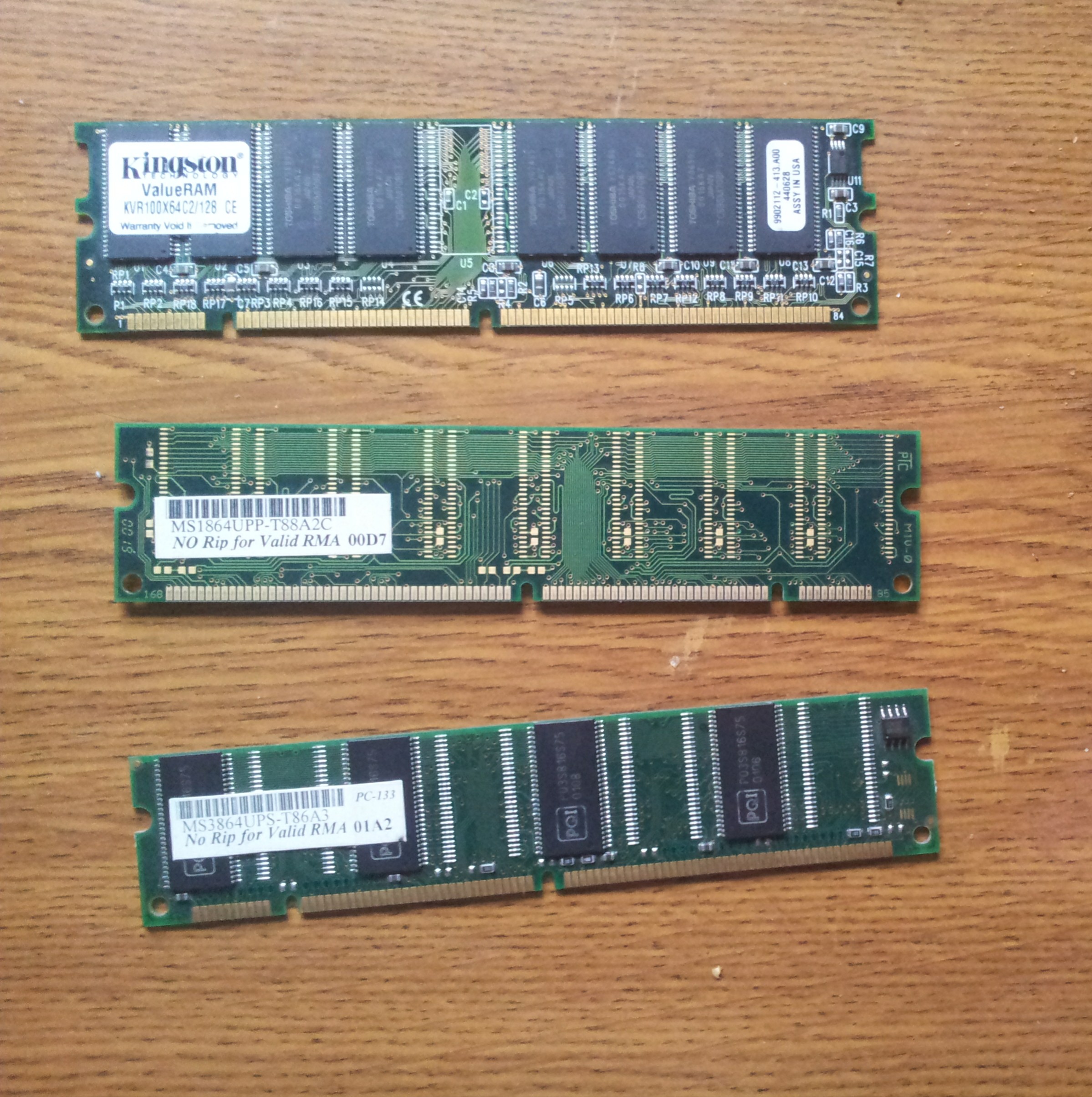
Synchronous dynamic random-access memory (synchronous dynamic RAM or SDRAM) is any DRAM where the operation of its external pin interface is coordinated by an externally supplied clock signal. DRAM integrated circuits (ICs) produced from the early 1970s to early 1990s used an ''asynchronous'' interface, in which input control signals have a direct effect on internal functions only delayed by the trip across its semiconductor pathways. SDRAM has a ''synchronous'' interface, whereby changes on control inputs are recognised after a rising edge of its clock input. In SDRAM families standardized by JEDEC, the clock signal controls the stepping of an internal finite-state machine that responds to incoming commands. These commands can be pipelined to improve performance, with previously started operations completing while new commands are received. The memory is divided into several equally sized but independent sections called ''banks'', allowing the device to operate on a memory acc ... [...More Info...] [...Related Items...] OR: [Wikipedia] [Google] [Baidu] |
TSMC
Taiwan Semiconductor Manufacturing Company Limited (TSMC; also called Taiwan Semiconductor) is a Taiwanese multinational semiconductor contract manufacturing and design company. It is the world's most valuable semiconductor company, the world's largest dedicated independent ( pure-play) semiconductor foundry, and one of Taiwan's largest companies, with its headquarters and main operations located in the Hsinchu Science Park in Hsinchu. It is majority owned by foreign investors. Founded in Taiwan in 1987 by Morris Chang, TSMC was the world's first dedicated semiconductor foundry and has long been the leading company in its field. When Chang retired in 2018, after 31 years of TSMC leadership, Mark Liu became chairman and C. C. Wei became Chief Executive. It has been listed on the Taiwan Stock Exchange (TWSE: 2330) since 1993; in 1997 it became the first Taiwanese company to be listed on the New York Stock Exchange (NYSE: TSM). Since 1994, TSMC has had a compound annual growth ... [...More Info...] [...Related Items...] OR: [Wikipedia] [Google] [Baidu] |


