|
Pad Cratering
Pad cratering is a mechanically induced fracture in the resin between copper foil and outermost layer of fiberglass of a printed circuit board (PCB). It may be within the resin or at the resin to fiberglass interface. The pad remains connected to the component (usually a Ball Grid Array, BGA) and leaves a "crater" on the surface of the printed circuit board. Overview Pad cratering most often occurs during dynamic mechanical events such as mechanical shock or board flexure due to In-circuit test (ICT), board depaneling, or connector insertion. However, pad cratering has also been known to occur during thermal shock or even thermal cycling. Susceptibility to pad cratering can be impacted by several factors such as: PCB thickness, PCB laminate material properties, component size and stiffness, component location, and solder alloy selection among other factors. Testing IPC-9708 provides three test methods to characterize the pad cratering of a component and PCBA: pin pull, ball pull, ... [...More Info...] [...Related Items...] OR: [Wikipedia] [Google] [Baidu] |
Fracture
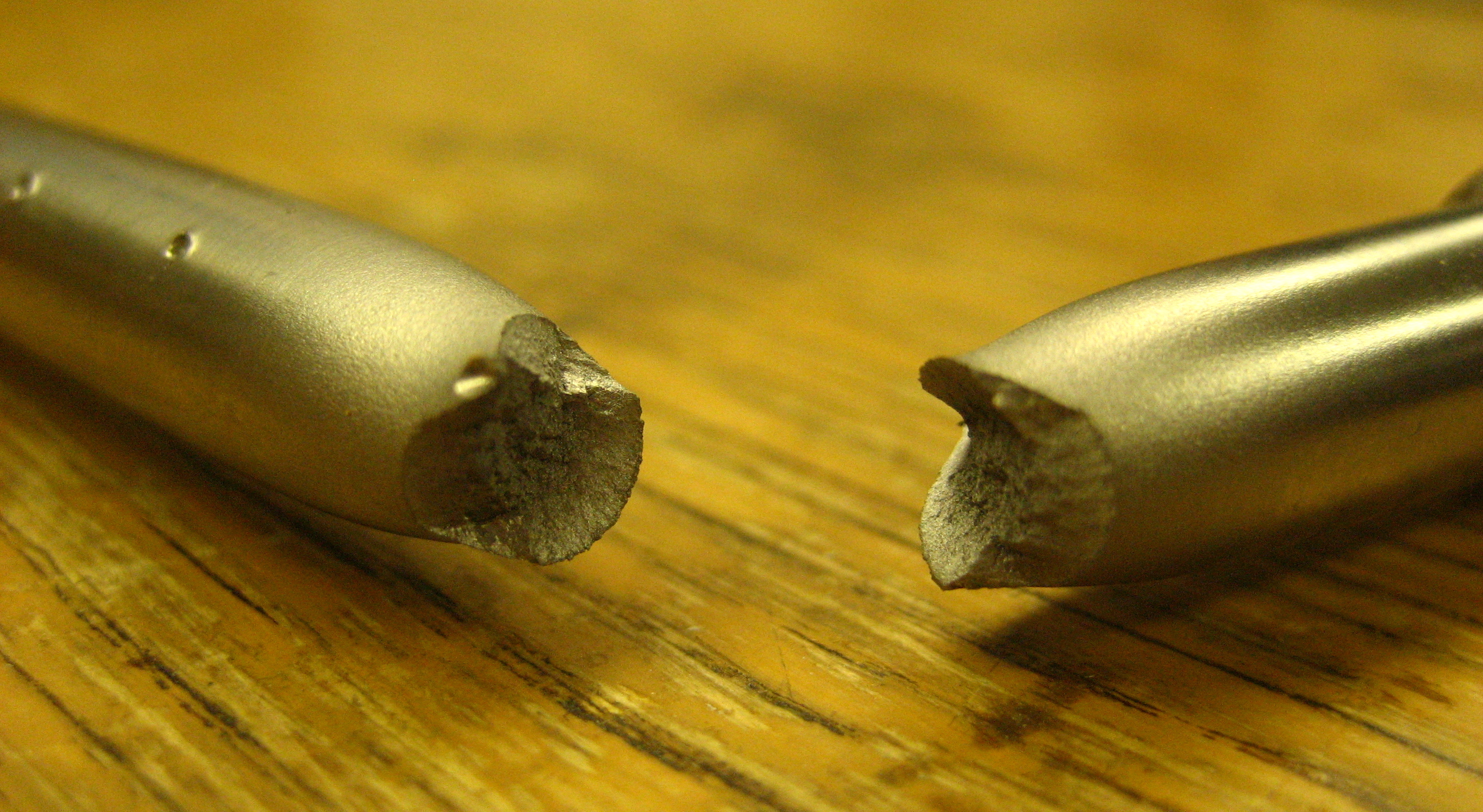
Fracture is the appearance of a crack or complete separation of an object or material into two or more pieces under the action of stress (mechanics), stress. The fracture of a solid usually occurs due to the development of certain displacement discontinuity surfaces within the solid. If a displacement develops perpendicular to the surface, it is called a normal tensile crack or simply a crack; if a displacement develops tangentially, it is called a shear crack, slip band, or dislocation. #Brittle, Brittle fractures occur without any apparent deformation before fracture. #Ductile, Ductile fractures occur after visible deformation. Fracture strength, or breaking strength, is the stress when a specimen fails or fractures. The detailed understanding of how a fracture occurs and develops in materials is the object of fracture mechanics. Strength Fracture strength, also known as breaking strength, is the stress at which a specimen structural integrity and failure, fails via fra ... [...More Info...] [...Related Items...] OR: [Wikipedia] [Google] [Baidu] |
X-ray Microscope
An X-ray microscope uses electromagnetic radiation in the X-ray band to produce magnified images of objects. Since X-rays penetrate most objects, there is no need to specially prepare them for X-ray microscopy observations. Unlike visible light, X-rays do not reflect or refract easily and are invisible to the human eye. Therefore, an X-ray microscope exposes film or uses a charge-coupled device (CCD) detector to detect X-rays that pass through the specimen. It is a contrast imaging technology using the difference in absorption of soft X-rays in the water window region (wavelengths: 2.34–4.4 nm, energies: 280–530 eV) by the carbon atom (main element composing the living cell) and the oxygen atom (an element of water). Microfocus X-ray also achieves high magnification by projection. A microfocus X-ray tube produces X-rays from an extremely small focal spot (5 μm down to 0.1 μm). The X-rays are in the more conventional X-ray range (20 to 300 keV) and ... [...More Info...] [...Related Items...] OR: [Wikipedia] [Google] [Baidu] |
Solder Ball
In integrated circuit packaging, a solder ball, also a solder bump (often referred to simply as "ball" or "bumps") is a ball of solder that provides the contact between the chip package and the printed circuit board, as well as between stacked packages in multichip modules; in the latter case, they may be referred to as microbumps (μbumps, ubumps), since they are usually significantly smaller than the former. The solder balls can be placed manually or by automated equipment, and are held in place with a tacky flux. A coined solder ball is a solder ball subject to coining, i.e., flattening to a shape resembling that of a coin, to increase contact reliability. Ball grid array, chip-scale package, and flip chip packages generally use solder balls. Underfill After the solder balls are used to attach an integrated circuit chip to a printed circuit board (PCB), often the remaining air gap between them is underfilled with epoxy. In some cases, there may be multiple layers of so ... [...More Info...] [...Related Items...] OR: [Wikipedia] [Google] [Baidu] |
Thermal Expansion
Thermal expansion is the tendency of matter to increase in length, area, or volume, changing its size and density, in response to an increase in temperature (usually excluding phase transitions). Substances usually contract with decreasing temperature (thermal contraction), with rare exceptions within limited temperature ranges ('' negative thermal expansion''). Temperature is a monotonic function of the average molecular kinetic energy of a substance. As energy in particles increases, they start moving faster and faster, weakening the intermolecular forces between them and therefore expanding the substance. When a substance is heated, molecules begin to vibrate and move more, usually creating more distance between themselves. The relative expansion (also called strain) divided by the change in temperature is called the material's coefficient of linear thermal expansion and generally varies with temperature. Prediction If an equation of state is available, it can be used t ... [...More Info...] [...Related Items...] OR: [Wikipedia] [Google] [Baidu] |
Young's Modulus
Young's modulus (or the Young modulus) is a mechanical property of solid materials that measures the tensile or compressive stiffness when the force is applied lengthwise. It is the modulus of elasticity for tension or axial compression. Young's modulus is defined as the ratio of the stress (force per unit area) applied to the object and the resulting axial strain (displacement or deformation) in the linear elastic region of the material. Although Young's modulus is named after the 19th-century British scientist Thomas Young, the concept was developed in 1727 by Leonhard Euler. The first experiments that used the concept of Young's modulus in its modern form were performed by the Italian scientist Giordano Riccati in 1782, pre-dating Young's work by 25 years. The term modulus is derived from the Latin root term '' modus'', which means ''measure''. Definition Young's modulus, E, quantifies the relationship between tensile or compressive stress \sigma (force per unit ar ... [...More Info...] [...Related Items...] OR: [Wikipedia] [Google] [Baidu] |
Yield (engineering)
In materials science and engineering, the yield point is the point on a stress–strain curve that indicates the limit of elastic behavior and the beginning of plastic behavior. Below the yield point, a material will deform elastically and will return to its original shape when the applied stress is removed. Once the yield point is passed, some fraction of the deformation will be permanent and non-reversible and is known as plastic deformation. The yield strength or yield stress is a material property and is the stress corresponding to the yield point at which the material begins to deform plastically. The yield strength is often used to determine the maximum allowable load in a mechanical component, since it represents the upper limit to forces that can be applied without producing permanent deformation. For most metals, such as aluminium and cold-worked steel, there is a gradual onset of non-linear behavior, and no precise yield point. In such a case, the offset yield p ... [...More Info...] [...Related Items...] OR: [Wikipedia] [Google] [Baidu] |
Plasticity (physics)
In physics and materials science, plasticity (also known as plastic deformation) is the ability of a solid material to undergo permanent Deformation (engineering), deformation, a non-reversible change of shape in response to applied forces. For example, a solid piece of metal being bent or pounded into a new shape displays plasticity as permanent changes occur within the material itself. In engineering, the transition from Elasticity (physics), elastic behavior to plastic behavior is known as Yield (engineering), yielding. Plastic deformation is observed in most materials, particularly metals, soils, Rock (geology), rocks, concrete, and foams. However, the physical mechanisms that cause plastic deformation can vary widely. At a crystalline scale, plasticity in metals is usually a consequence of dislocations. Such defects are relatively rare in most crystalline materials, but are numerous in some and part of their crystal structure; in such cases, plastic crystallinity can resul ... [...More Info...] [...Related Items...] OR: [Wikipedia] [Google] [Baidu] |
Creep (deformation)
In materials science, creep (sometimes called cold flow) is the tendency of a solid material to undergo slow deformation while subject to persistent mechanical stresses. It can occur as a result of long-term exposure to high levels of stress that are still below the yield strength of the material. Creep is more severe in materials that are subjected to heat for long periods and generally increases as they near their melting point. The rate of deformation is a function of the material's properties, exposure time, exposure temperature and the applied structural load. Depending on the magnitude of the applied stress and its duration, the deformation may become so large that a component can no longer perform its function – for example creep of a turbine blade could cause the blade to contact the casing, resulting in the failure of the blade. Creep is usually of concern to engineers and metallurgists when evaluating components that operate under high stresses or high temperatures ... [...More Info...] [...Related Items...] OR: [Wikipedia] [Google] [Baidu] |
Physics Of Failure
Physics of failure is a technique under the practice of reliability design that leverages the knowledge and understanding of the processes and mechanisms that induce failure to predict reliability and improve product performance. Other definitions of Physics of Failure include: * A science-based approach to reliability that uses modeling and simulation to design-in reliability. It helps to understand system performance and reduce decision risk during design and after the equipment is fielded. This approach models the root causes of failure such as fatigue, fracture, wear, and corrosion. * An approach to the design and development of reliable product to prevent failure, based on the knowledge of root cause failure mechanisms. The Physics of Failure (PoF) concept is based on the understanding of the relationships between requirements and the physical characteristics of the product and their variation in the manufacturing processes, and the reaction of product elements and materials t ... [...More Info...] [...Related Items...] OR: [Wikipedia] [Google] [Baidu] |
Finite Element Analysis
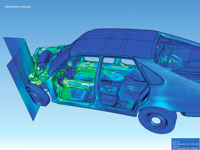
Finite element method (FEM) is a popular method for numerically solving differential equations arising in engineering and mathematical models, mathematical modeling. Typical problem areas of interest include the traditional fields of structural analysis, heat transfer, fluid flow, mass transport, and electromagnetic potential. Computers are usually used to perform the calculations required. With high-speed supercomputers, better solutions can be achieved and are often required to solve the largest and most complex problems. FEM is a general numerical analysis, numerical method for solving partial differential equations in two- or three-space variables (i.e., some boundary value problems). There are also studies about using FEM to solve high-dimensional problems. To solve a problem, FEM subdivides a large system into smaller, simpler parts called finite elements. This is achieved by a particular space discretization in the space dimensions, which is implemented by the constructio ... [...More Info...] [...Related Items...] OR: [Wikipedia] [Google] [Baidu] |
Scanning Electron Microscope
A scanning electron microscope (SEM) is a type of electron microscope that produces images of a sample by scanning the surface with a focused beam of electrons. The electrons interact with atoms in the sample, producing various signals that contain information about the surface topography and composition. The electron beam is scanned in a raster scan pattern, and the position of the beam is combined with the intensity of the detected signal to produce an image. In the most common SEM mode, secondary electrons emitted by atoms excited by the electron beam are detected using a secondary electron detector ( Everhart–Thornley detector). The number of secondary electrons that can be detected, and thus the signal intensity, depends, among other things, on specimen topography. Some SEMs can achieve resolutions better than 1 nanometer. Specimens are observed in high vacuum in a conventional SEM, or in low vacuum or wet conditions in a variable pressure or environmental SEM, an ... [...More Info...] [...Related Items...] OR: [Wikipedia] [Google] [Baidu] |
Destructive Testing
In destructive testing (or destructive physical analysis, DPA) tests are carried out to the specimen's failure, in order to understand a specimen's performance or material behavior under different loads. These tests are generally much easier to carry out, yield more information, and are easier to interpret than nondestructive testing. Applications Destructive testing is most suitable, and economic, for objects which will be mass-produced, as the cost of destroying a small number of specimens is negligible. It is usually not economical to do destructive testing where only one or very few items are to be produced (for example, in the case of a building). Analyzing and documenting destructive failure mode Analyzing and documenting the destructive failure mode is often accomplished using a high-speed camera recording continuously (movie-loop) until the failure is detected. Detecting the failure can be accomplished using a sound detector or stress gauge which produces a signal to tri ... [...More Info...] [...Related Items...] OR: [Wikipedia] [Google] [Baidu] |


