|
Optoelectrowetting
Optoelectrowetting (OEW) is a method of liquid droplet manipulation used in microfluidics applications. This technique builds on the principle of electrowetting, which has proven useful in liquid actuation due to fast switching response times and low power consumption. Where traditional electrowetting runs into challenges, however, such as in the simultaneous manipulation of multiple droplets, OEW presents a lucrative alternative that is both simpler and cheaper to produce. OEW surfaces are easy to fabricate, since they require no lithography, and have real-time, reconfigurable, large-scale manipulation control, due to its reaction to light intensity. Theory The traditional electrowetting mechanism has been receiving increasing interest due to its ability to control tension forces on a liquid droplet. As surface tension acts as the dominant liquid actuation force in nano-scale applications, electrowetting has been used to modify this tension at the solid-liquid interface through ... [...More Info...] [...Related Items...] OR: [Wikipedia] [Google] [Baidu] |
Electrowetting
Electrowetting is the modification of the wetting properties of a surface (which is typically hydrophobic) with an applied electric field. History The electrowetting of mercury and other liquids on variably charged surfaces was probably first explained by Gabriel Lippmann in 1875 and was certainly observed much earlier. A. N. Frumkin used surface charge to change the shape of water drops in 1936. The term electrowetting was first introduced in 1981 by G. Beni and S. Hackwood to describe an effect proposed for designing a new type of display device for which they received a patent. The use of a "fluid transistor" in microfluidic circuits for manipulating chemical and biological fluids was first investigated by J. Brown in 1980 and later funded in 1984–1988 under NSF Grants 8760730 & 8822197, employing insulating dielectric and hydrophobic layer(s) (EWOD), immiscible fluids, DC or RF power; and mass arrays of miniature interleaved (saw tooth) electrodes with large or matching In ... [...More Info...] [...Related Items...] OR: [Wikipedia] [Google] [Baidu] |
Photoelectrowetting
Photoelectrowetting is a modification of the wetting properties of a surface (typically a hydrophobic surface) using incident light. Working principle Whereas ordinary electrowetting is observed in surfaces consisting of a liquid/ insulator/conductor stack, photoelectrowetting can be observed by replacing the conductor with a semiconductor to form a liquid/insulator/semiconductor stack. This has electrical and optical properties similar to the metal/insulator/semiconductor stack used in metal-oxide-semiconductor field effect transistors (MOSFETs) and charge-coupled devices (CCDs). Replacing the conductor with a semiconductor results in asymmetrical electrowetting behavior (in terms of voltage polarity), depending on the semiconductor doping type and density. Incident light above the semiconductor's band gap creates photo-induced carriers via electron-hole pair generation in the depletion region of the underlying semiconductor. This leads to a modification of the capacitance of ... [...More Info...] [...Related Items...] OR: [Wikipedia] [Google] [Baidu] |
Microfluidics
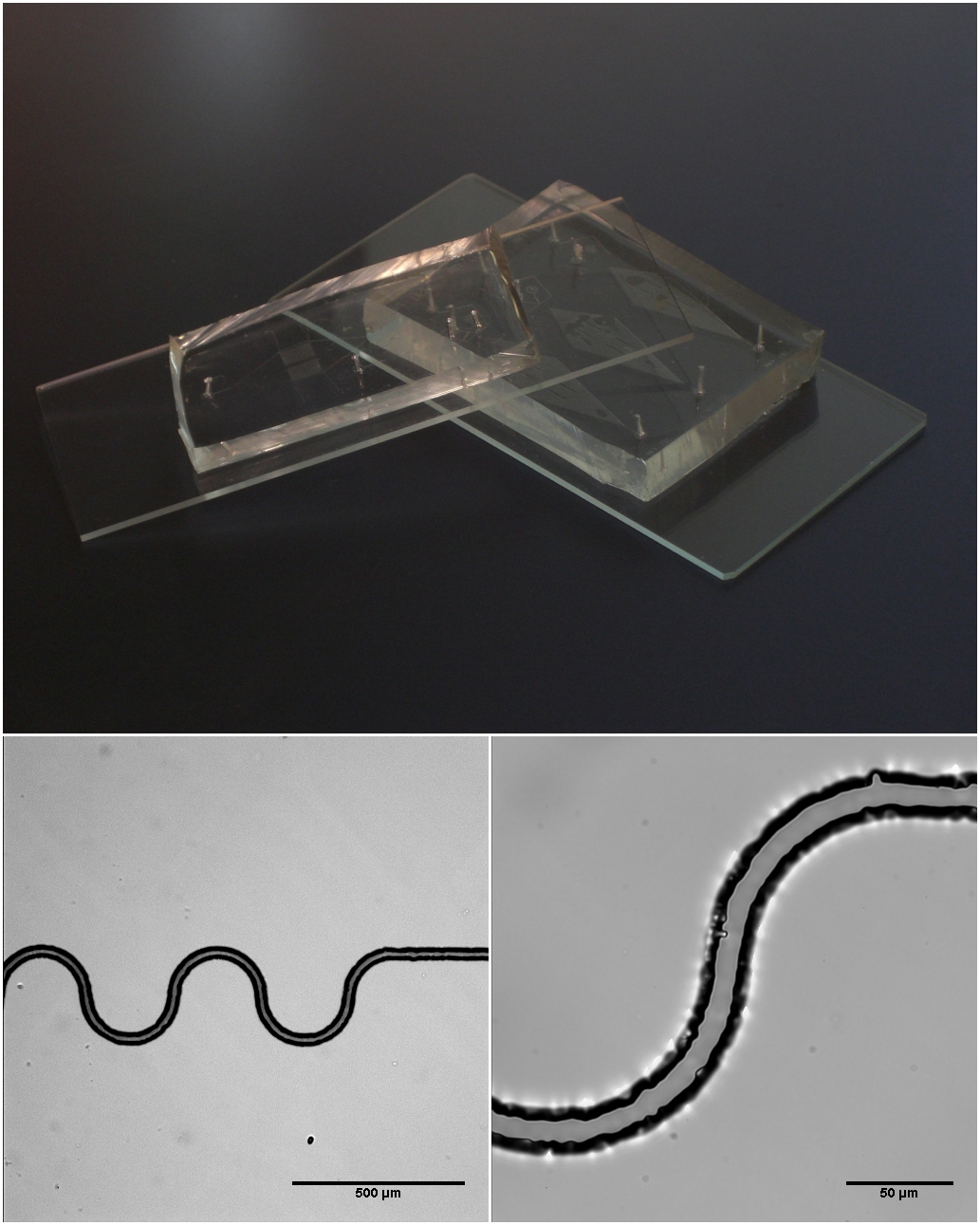
Microfluidics refers to the behavior, precise control, and manipulation of fluids that are geometrically constrained to a small scale (typically sub-millimeter) at which surface forces dominate volumetric forces. It is a multidisciplinary field that involves engineering, physics, chemistry, biochemistry, nanotechnology, and biotechnology. It has practical applications in the design of systems that process low volumes of fluids to achieve multiplexing, automation, and high-throughput screening. Microfluidics emerged in the beginning of the 1980s and is used in the development of inkjet printheads, DNA chips, lab-on-a-chip technology, micro-propulsion, and micro-thermal technologies. Typically, micro means one of the following features: * Small volumes (μL, nL, pL, fL) * Small size * Low energy consumption * Microdomain effects Typically microfluidic systems transport, mix, separate, or otherwise process fluids. Various applications rely on passive fluid control using capillary ... [...More Info...] [...Related Items...] OR: [Wikipedia] [Google] [Baidu] |
Nanotechnology
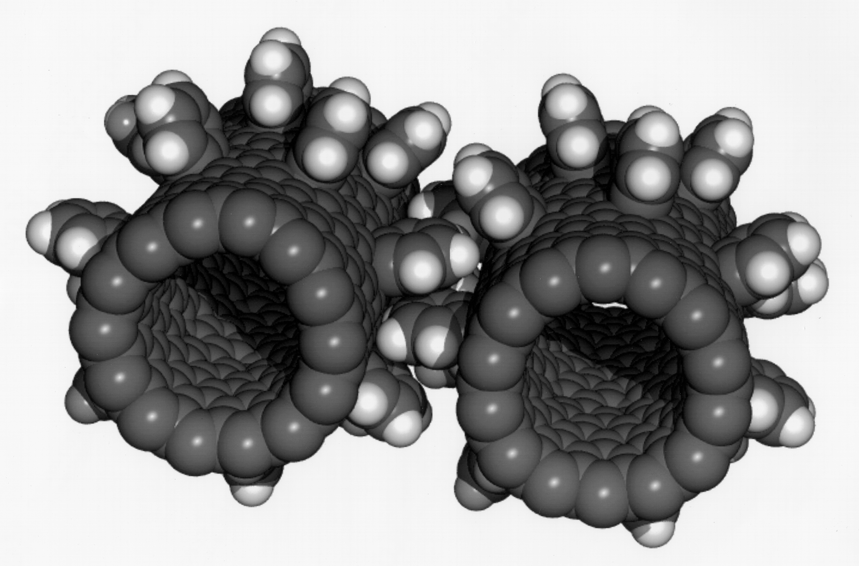
Nanotechnology, also shortened to nanotech, is the use of matter on an atomic, molecular, and supramolecular scale for industrial purposes. The earliest, widespread description of nanotechnology referred to the particular technological goal of precisely manipulating atoms and molecules for fabrication of macroscale products, also now referred to as molecular nanotechnology. A more generalized description of nanotechnology was subsequently established by the National Nanotechnology Initiative, which defined nanotechnology as the manipulation of matter with at least one dimension sized from 1 to 100 nanometers (nm). This definition reflects the fact that quantum mechanical effects are important at this quantum-realm scale, and so the definition shifted from a particular technological goal to a research category inclusive of all types of research and technologies that deal with the special properties of matter which occur below the given size threshold. It is therefore commo ... [...More Info...] [...Related Items...] OR: [Wikipedia] [Google] [Baidu] |
Fluid Dynamics
In physics and engineering, fluid dynamics is a subdiscipline of fluid mechanics that describes the flow of fluids—liquids and gases. It has several subdisciplines, including '' aerodynamics'' (the study of air and other gases in motion) and hydrodynamics (the study of liquids in motion). Fluid dynamics has a wide range of applications, including calculating forces and moments on aircraft, determining the mass flow rate of petroleum through pipelines, predicting weather patterns, understanding nebulae in interstellar space and modelling fission weapon detonation. Fluid dynamics offers a systematic structure—which underlies these practical disciplines—that embraces empirical and semi-empirical laws derived from flow measurement and used to solve practical problems. The solution to a fluid dynamics problem typically involves the calculation of various properties of the fluid, such as flow velocity, pressure, density, and temperature, as functions of space a ... [...More Info...] [...Related Items...] OR: [Wikipedia] [Google] [Baidu] |
Microelectromechanical Systems
Microelectromechanical systems (MEMS), also written as micro-electro-mechanical systems (or microelectronic and microelectromechanical systems) and the related micromechatronics and microsystems constitute the technology of microscopic devices, particularly those with moving parts. They merge at the nanoscale into nanoelectromechanical systems (NEMS) and nanotechnology. MEMS are also referred to as micromachines in Japan and microsystem technology (MST) in Europe. MEMS are made up of components between 1 and 100 micrometers in size (i.e., 0.001 to 0.1 mm), and MEMS devices generally range in size from 20 micrometres to a millimetre (i.e., 0.02 to 1.0 mm), although components arranged in arrays (e.g., digital micromirror devices) can be more than 1000 mm2. They usually consist of a central unit that processes data (an integrated circuit chip such as microprocessor) and several components that interact with the surroundings (such as microsensors). Because of th ... [...More Info...] [...Related Items...] OR: [Wikipedia] [Google] [Baidu] |
Lab-on-a-chip
A lab-on-a-chip (LOC) is a device that integrates one or several laboratory functions on a single integrated circuit (commonly called a "chip") of only millimeters to a few square centimeters to achieve automation and high-throughput screening. LOCs can handle extremely small fluid volumes down to less than pico-liters. Lab-on-a-chip devices are a subset of microelectromechanical systems (MEMS) devices and sometimes called "micro total analysis systems" (µTAS). LOCs may use microfluidics, the physics, manipulation and study of minute amounts of fluids. However, strictly regarded "lab-on-a-chip" indicates generally the scaling of single or multiple lab processes down to chip-format, whereas "µTAS" is dedicated to the integration of the total sequence of lab processes to perform chemical analysis. The term "lab-on-a-chip" was introduced when it turned out that µTAS technologies were applicable for more than only analysis purposes. History After the invention of microtechno ... [...More Info...] [...Related Items...] OR: [Wikipedia] [Google] [Baidu] |
Charge-coupled Device
A charge-coupled device (CCD) is an integrated circuit containing an array of linked, or coupled, capacitors. Under the control of an external circuit, each capacitor can transfer its electric charge to a neighboring capacitor. CCD sensors are a major technology used in digital imaging. In a CCD image sensor, pixels are represented by p-doped metal–oxide–semiconductor (MOS) capacitors. These MOS capacitors, the basic building blocks of a CCD, are biased above the threshold for inversion when image acquisition begins, allowing the conversion of incoming photons into electron charges at the semiconductor-oxide interface; the CCD is then used to read out these charges. Although CCDs are not the only technology to allow for light detection, CCD image sensors are widely used in professional, medical, and scientific applications where high-quality image data are required. In applications with less exacting quality demands, such as consumer and professional digital camera ... [...More Info...] [...Related Items...] OR: [Wikipedia] [Google] [Baidu] |
Photodiode
A photodiode is a light-sensitive semiconductor diode. It produces current when it absorbs photons. The package of a photodiode allows light (or infrared or ultraviolet radiation, or X-rays) to reach the sensitive part of the device. The package may include lenses or optical filters. Devices designed for use specially as a photodiode use a PIN junction rather than a p–n junction, to increase the speed of response. Photodiodes usually have a slower response time as their surface area increases. A photodiode is designed to operate in reverse bias. A solar cell used to generate electric solar power is a large area photodiode. Photodiodes are used in scientific and industrial instruments to measure light intensity, either for its own sake or as a measure of some other property (density of smoke, for example). A photodiode can be used as the receiver of data encoded on an infrared beam, as in household remote controls. Photodiodes can be used to form an optocoupler, allowing ... [...More Info...] [...Related Items...] OR: [Wikipedia] [Google] [Baidu] |
Space Charge
Space charge is an interpretation of a collection of electric charges in which excess electric charge is treated as a continuum of charge distributed over a region of space (either a volume or an area) rather than distinct point-like charges. This model typically applies when charge carriers have been emitted from some region of a solid—the cloud of emitted carriers can form a space charge region if they are sufficiently spread out, or the charged atoms or molecules left behind in the solid can form a space charge region. Space charge only occurs in dielectric media (including vacuum) because in a conductive medium the charge tends to be rapidly neutralized or screened. The sign of the space charge can be either negative or positive. This situation is perhaps most familiar in the area near a metal object when it is heated to incandescence in a vacuum. This effect was first observed by Thomas Edison in light bulb filaments, where it is sometimes called the Edison effect. Space ... [...More Info...] [...Related Items...] OR: [Wikipedia] [Google] [Baidu] |
Charge Carrier
In physics, a charge carrier is a particle or quasiparticle that is free to move, carrying an electric charge, especially the particles that carry electric charges in electrical conductors. Examples are electrons, ions and holes. The term is used most commonly in solid state physics. In a conducting medium, an electric field can exert force on these free particles, causing a net motion of the particles through the medium; this is what constitutes an electric current. In conducting media, particles serve to carry charge: *In many metals, the charge carriers are electrons. One or two of the valence electrons from each atom are able to move about freely within the crystal structure of the metal. The free electrons are referred to as conduction electrons, and the cloud of free electrons is called a Fermi gas. Many metals have electron and hole bands. In some, the majority carriers are holes. *In electrolytes, such as salt water, the charge carriers are ions, which are atoms ... [...More Info...] [...Related Items...] OR: [Wikipedia] [Google] [Baidu] |


