|
Multi-tip Scanning Tunneling Microscopy
Multi-tip scanning tunneling microscopy (Multi-tip STM) extends ''scanning tunneling microscopy'' (STM) from imaging to dedicated electrical measurements at the nanoscale like a ″multimeter at the nanoscale″. In materials science, nanoscience, and nanotechnology, it is desirable to measure electrical properties at a particular position of the sample. For this purpose, multi-tip STMs in which several tips are operated independently have been developed. Apart from imaging the sample, the tips of a multi-tip STM are used to form contacts to the sample at desired locations and to perform local electrical measurements. Introduction As microelectronics evolves into nanoelectronics, it is essential to perform electronic transport measurements at nanoscale. The standard approach is to use lithographic methods to contact nanostructures, as it is also used in the final nanoelectronic device. In research and development stages, however, other methods to contact nanoelectronic devices o ... [...More Info...] [...Related Items...] OR: [Wikipedia] [Google] [Baidu] |
Nanowires
A nanowire is a nanostructure in the form of a wire with the diameter of the order of a nanometre (10−9 metres). More generally, nanowires can be defined as structures that have a thickness or diameter constrained to tens of nanometers or less and an unconstrained length. At these scales, quantum mechanical effects are important—which coined the term "quantum wires". Many different types of nanowires exist, including superconducting (e.g. YBCO), metallic (e.g. Ni, Pt, Au, Ag), semiconducting (e.g. silicon nanowires (SiNWs), InP, GaN) and insulating (e.g. SiO2, TiO2). Molecular nanowires are composed of repeating molecular units either organic (e.g. DNA) or inorganic (e.g. Mo6S9−xIx). Characteristics upright=1.2, Crystalline 2×2-atom tin selenide nanowire grown inside a single-wall carbon nanotube (tube diameter ~1 nm). file:[email protected], A noise-filtered HRTEM image of a HgTe extreme nanowire embedded down the central pore of a SWCNT. The image is also accom ... [...More Info...] [...Related Items...] OR: [Wikipedia] [Google] [Baidu] |
Nanoprobing
Nanoprobing is method of extracting device electrical parameters through the use of nanoscale tungsten wires, used primarily in the semiconductor industry. The characterization of individual devices is instrumental to engineers and integrated circuit designers during initial product development and debug. It is commonly utilized in device failure analysis laboratories to aid with yield enhancement, quality and reliability issues and customer returns. Commercially available nanoprobing systems are integrated into either a vacuum-based scanning electron microscope (SEM) or atomic force microscope (AFM). Nanoprobing systems that are based on AFM technology are referred to as Atomic Force nanoProbers (AFP). Principles and operation AFM based nanoprobers, enable up to eight probe tips to be scanned to generate high resolution AFM topography images, as well as Conductive AFM, Scanning Capacitance, and Electrostatic Force Microscopy images. Conductive AFM provides pico-amp resolution ... [...More Info...] [...Related Items...] OR: [Wikipedia] [Google] [Baidu] |
Atomic Force Microscopy
Atomic force microscopy (AFM) or scanning force microscopy (SFM) is a very-high-resolution type of scanning probe microscopy (SPM), with demonstrated resolution on the order of fractions of a nanometer, more than 1000 times better than the optical diffraction limit. Overview Atomic force microscopy (AFM) is a type of scanning probe microscopy (SPM), with demonstrated resolution on the order of fractions of a nanometer, more than 1000 times better than the optical diffraction limit. The information is gathered by "feeling" or "touching" the surface with a mechanical probe. Piezoelectric elements that facilitate tiny but accurate and precise movements on (electronic) command enable precise scanning. Despite the name, the Atomic Force Microscope does not use the Nuclear force. Abilities The AFM has three major abilities: force measurement, topographic imaging, and manipulation. In force measurement, AFMs can be used to measure the forces between the probe and the sample as ... [...More Info...] [...Related Items...] OR: [Wikipedia] [Google] [Baidu] |
Scanning Tunneling Microscopy
A scanning tunneling microscope (STM) is a type of microscope used for imaging surfaces at the atomic level. Its development in 1981 earned its inventors, Gerd Binnig and Heinrich Rohrer, then at IBM Zürich, the Nobel Prize in Physics in 1986. STM senses the surface by using an extremely sharp conducting tip that can distinguish features smaller than 0.1 nm with a 0.01 nm (10 pm) depth resolution. This means that individual atoms can routinely be imaged and manipulated. Most microscopes are built for use in ultra-high vacuum at temperatures approaching zero kelvin, but variants exist for studies in air, water and other environments, and for temperatures over 1000 °C. STM is based on the concept of quantum tunneling. When the tip is brought very near to the surface to be examined, a bias voltage applied between the two allows electrons to tunnel through the vacuum separating them. The resulting ''tunneling current'' is a function of the tip position, appl ... [...More Info...] [...Related Items...] OR: [Wikipedia] [Google] [Baidu] |
Topological Insulator
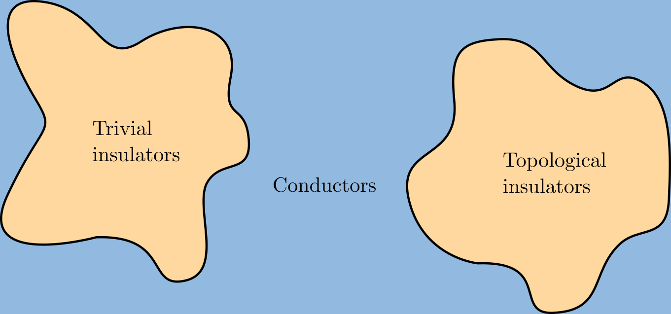
A topological insulator is a material whose interior behaves as an electrical insulator while its surface behaves as an electrical conductor, meaning that electrons can only move along the surface of the material. A topological insulator is an insulator for the same reason a " trivial" (ordinary) insulator is: there exists an energy gap between the valence and conduction bands of the material. But in a topological insulator, these bands are, in an informal sense, "twisted", relative to a trivial insulator. The topological insulator cannot be continuously transformed into a trivial one without untwisting the bands, which closes the band gap and creates a conducting state. Thus, due to the continuity of the underlying field, the border of a topological insulator with a trivial insulator (including vacuum, which is topologically trivial) is forced to support a conducting state. Since this results from a global property of the topological insulator's band structure, local (sym ... [...More Info...] [...Related Items...] OR: [Wikipedia] [Google] [Baidu] |


