|
Lattice Parameter
A lattice constant or lattice parameter is one of the physical dimensions and angles that determine the geometry of the unit cells in a crystal lattice, and is proportional to the distance between atoms in the crystal. A simple cubic crystal has only one lattice constant, the distance between atoms, but, in general, lattices in three dimensions have six lattice constants: the lengths ''a'', ''b'', and ''c'' of the three cell edges meeting at a vertex, and the angles ''α'', ''β'', and ''γ'' between those edges. The crystal lattice parameters ''a'', ''b'', and ''c'' have the dimension of length. The three numbers represent the size of the unit cell, that is, the distance from a given atom to an identical atom in the same position and orientation in a neighboring cell (except for very simple crystal structures, this will not necessarily be distance to the nearest neighbor). Their SI unit is the meter, and they are traditionally specified in angstroms (Å); an angstrom being 0.1 ... [...More Info...] [...Related Items...] OR: [Wikipedia] [Google] [Baidu] |
Stress (mechanics)
In continuum mechanics, stress is a physical quantity that describes forces present during deformation. For example, an object being pulled apart, such as a stretched elastic band, is subject to ''tensile'' stress and may undergo elongation. An object being pushed together, such as a crumpled sponge, is subject to ''compressive'' stress and may undergo shortening. The greater the force and the smaller the cross-sectional area of the body on which it acts, the greater the stress. Stress has dimension of force per area, with SI units of newtons per square meter (N/m2) or pascal (Pa). Stress expresses the internal forces that neighbouring particles of a continuous material exert on each other, while ''strain'' is the measure of the relative deformation of the material. For example, when a solid vertical bar is supporting an overhead weight, each particle in the bar pushes on the particles immediately below it. When a liquid is in a closed container under pressure, each ... [...More Info...] [...Related Items...] OR: [Wikipedia] [Google] [Baidu] |
Semiconductor Material
A semiconductor is a material with electrical conductivity between that of a Electrical conductor, conductor and an Insulator (electricity), insulator. Its conductivity can be modified by adding impurities ("doping (semiconductor), doping") to its crystal structure. When two regions with different doping levels are present in the same crystal, they form a semiconductor junction. The behavior of charge carriers, which include electrons, ions, and electron holes, at these junctions is the basis of diodes, transistors, and most modern electronics. Some examples of semiconductors are silicon, germanium, gallium arsenide, and elements near the so-called "metalloid staircase" on the periodic table. After silicon, gallium arsenide is the second-most common semiconductor and is used in laser diodes, solar cells, microwave-frequency integrated circuits, and others. Silicon is a critical element for fabricating most electronic circuits. Semiconductor devices can display a range of diffe ... [...More Info...] [...Related Items...] OR: [Wikipedia] [Google] [Baidu] |
Triple Product
In geometry and algebra, the triple product is a product of three 3- dimensional vectors, usually Euclidean vectors. The name "triple product" is used for two different products, the scalar-valued scalar triple product and, less often, the vector-valued vector triple product. Scalar triple product The scalar triple product (also called the mixed product, box product, or triple scalar product) is defined as the dot product of one of the vectors with the cross product of the other two. Geometric interpretation Geometrically, the scalar triple product : \mathbf\cdot(\mathbf\times \mathbf) is the (signed) volume of the parallelepiped defined by the three vectors given. Properties * The scalar triple product is unchanged under a circular shift of its three operands (a, b, c): *: \mathbf\cdot(\mathbf\times \mathbf)= \mathbf\cdot(\mathbf\times \mathbf)= \mathbf\cdot(\mathbf\times \mathbf) * Swapping the positions of the operators without re-ordering the operands ... [...More Info...] [...Related Items...] OR: [Wikipedia] [Google] [Baidu] |
Epitaxy
Epitaxy (prefix ''epi-'' means "on top of”) is a type of crystal growth or material deposition in which new crystalline layers are formed with one or more well-defined orientations with respect to the crystalline seed layer. The deposited crystalline film is called an epitaxial film or epitaxial layer. The relative orientation(s) of the epitaxial layer to the seed layer is defined in terms of the orientation of the crystal lattice of each material. For most epitaxial growths, the new layer is usually crystalline and each crystallographic domain of the overlayer must have a well-defined orientation relative to the substrate crystal structure. Epitaxy can involve single-crystal structures, although grain-to-grain epitaxy has been observed in granular films. For most technological applications, single-domain epitaxy, which is the growth of an overlayer crystal with one well-defined orientation with respect to the substrate crystal, is preferred. Epitaxy can also play an important ... [...More Info...] [...Related Items...] OR: [Wikipedia] [Google] [Baidu] |
Atomic Force Microscope
Atomic force microscopy (AFM) or scanning force microscopy (SFM) is a very-high-resolution type of scanning probe microscopy (SPM), with demonstrated resolution on the order of fractions of a nanometer, more than 1000 times better than the diffraction-limited system, optical diffraction limit. Overview Atomic force microscopy (AFM) gathers information by "feeling" or "touching" the surface with a mechanical probe. Piezoelectric elements that facilitate tiny but accurate and precise movements on (electronic) command enable precise scanning. Despite the name, the Atomic Force Microscope does not use the nuclear force. Abilities and spatial resolution The AFM has three major abilities: force measurement, topographic imaging, and manipulation. In force measurement, AFMs can be used to measure the forces between the probe and the sample as a function of their mutual separation. This can be applied to perform force spectroscopy, to measure the mechanical properties of the sample, s ... [...More Info...] [...Related Items...] OR: [Wikipedia] [Google] [Baidu] |
X-ray Diffraction
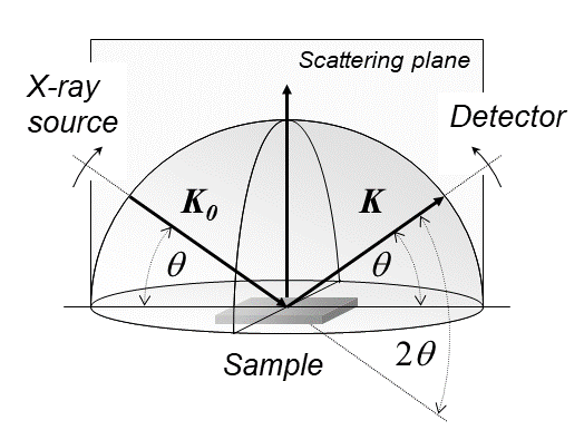
X-ray diffraction is a generic term for phenomena associated with changes in the direction of X-ray beams due to interactions with the electrons around atoms. It occurs due to elastic scattering, when there is no change in the energy of the waves. The resulting map of the directions of the X-rays far from the sample is called a diffraction pattern. It is different from X-ray crystallography which exploits X-ray diffraction to determine the arrangement of atoms in materials, and also has other components such as ways to map from experimental diffraction measurements to the positions of atoms. This article provides an overview of X-ray diffraction, starting with the early #History, history of x-rays and the discovery that they have the right spacings to be diffracted by crystals. In many cases these diffraction patterns can be #Introduction to x-ray diffraction theory, Interpreted using a single scattering or kinematical theory with conservation of energy (#Ewald's sphere, wave vecto ... [...More Info...] [...Related Items...] OR: [Wikipedia] [Google] [Baidu] |
Hexagonal Crystal System
In crystallography, the hexagonal crystal family is one of the six crystal family, crystal families, which includes two crystal systems (hexagonal and trigonal) and two lattice systems (hexagonal and rhombohedral). While commonly confused, the trigonal crystal system and the rhombohedral lattice system are not equivalent (see section hexagonal crystal family#Crystal systems, crystal systems below). In particular, there are crystals that have trigonal symmetry but belong to the hexagonal lattice (such as α-quartz). The hexagonal crystal family consists of the 12 point groups such that at least one of their space groups has the hexagonal lattice as underlying lattice, and is the union of the hexagonal crystal system and the trigonal crystal system. There are 52 space groups associated with it, which are exactly those whose Bravais lattice is either hexagonal or rhombohedral. __TOC__ Lattice systems The hexagonal crystal family consists of two lattice systems: hexagonal and rhom ... [...More Info...] [...Related Items...] OR: [Wikipedia] [Google] [Baidu] |
Kelvin
The kelvin (symbol: K) is the base unit for temperature in the International System of Units (SI). The Kelvin scale is an absolute temperature scale that starts at the lowest possible temperature (absolute zero), taken to be 0 K. By definition, the Celsius scale (symbol °C) and the Kelvin scale have the exact same magnitude; that is, a rise of 1 K is equal to a rise of 1 °C and vice versa, and any temperature in degrees Celsius can be converted to kelvin by adding 273.15. The 19th century British scientist Lord Kelvin first developed and proposed the scale. It was often called the "absolute Celsius" scale in the early 20th century. The kelvin was formally added to the International System of Units in 1954, defining 273.16 K to be the triple point of water. The Celsius, Fahrenheit, and Rankine scales were redefined in terms of the Kelvin scale using this definition. The 2019 revision of the SI now defines the kelvin in terms of energy by setting the Bo ... [...More Info...] [...Related Items...] OR: [Wikipedia] [Google] [Baidu] |
Diamond
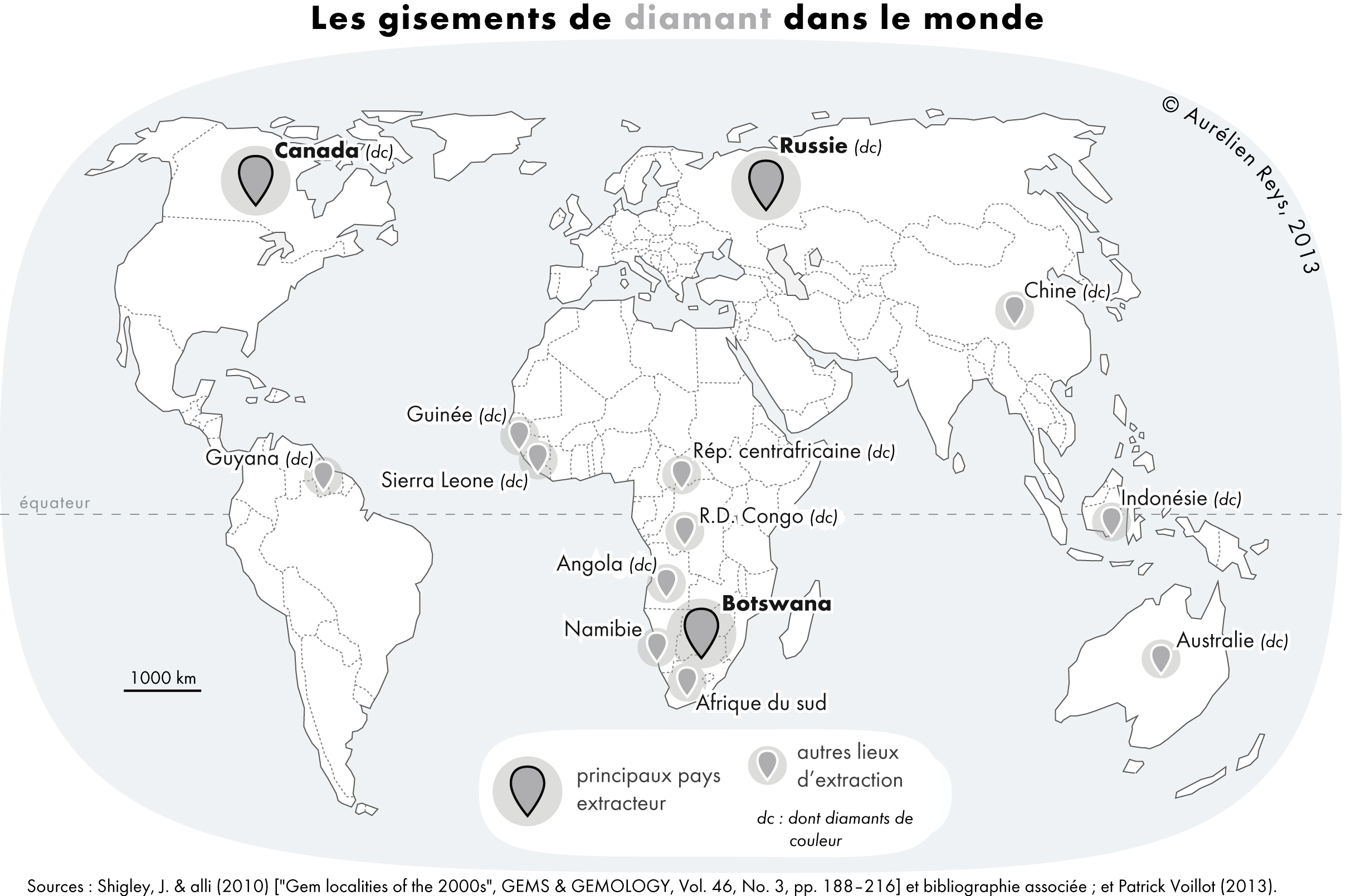
Diamond is a Allotropes of carbon, solid form of the element carbon with its atoms arranged in a crystal structure called diamond cubic. Diamond is tasteless, odourless, strong, brittle solid, colourless in pure form, a poor conductor of electricity, and insoluble in water. Another solid form of carbon known as graphite is the Chemical stability, chemically stable form of carbon at Standard temperature and pressure, room temperature and pressure, but diamond is metastable and converts to it at a negligible rate under those conditions. Diamond has the highest Scratch hardness, hardness and thermal conductivity of any natural material, properties that are used in major industrial applications such as cutting and polishing tools. Because the arrangement of atoms in diamond is extremely rigid, few types of impurity can contaminate it (two exceptions are boron and nitrogen). Small numbers of lattice defect, defects or impurities (about one per million of lattice atoms) can color ... [...More Info...] [...Related Items...] OR: [Wikipedia] [Google] [Baidu] |
Cubic Crystal System
In crystallography, the cubic (or isometric) crystal system is a crystal system where the unit cell is in the shape of a cube. This is one of the most common and simplest shapes found in crystals and minerals. There are three main varieties of these crystals: *Primitive cubic (abbreviated ''cP'' and alternatively called simple cubic) *Body-centered cubic (abbreviated ''cI'' or bcc) *Face-centered cubic (abbreviated ''cF'' or fcc) Note: the term fcc is often used in synonym for the ''cubic close-packed'' or ccp structure occurring in metals. However, fcc stands for a face-centered cubic Bravais lattice, which is not necessarily close-packed when a motif is set onto the lattice points. E.g. the diamond and the zincblende lattices are fcc but not close-packed. Each is subdivided into other variants listed below. Although the ''unit cells'' in these crystals are conventionally taken to be cubes, the primitive unit cells often are not. Bravais lattices The three Bravais latices ... [...More Info...] [...Related Items...] OR: [Wikipedia] [Google] [Baidu] |
Crystal Defect
A crystallographic defect is an interruption of the regular patterns of arrangement of atoms or molecules in crystalline solids. The positions and orientations of particles, which are repeating at fixed distances determined by the unit cell parameters in crystals, exhibit a periodic crystal structure, but this is usually imperfect.Ehrhart, P. (1991Properties and interactions of atomic defects in metals and alloys, volume 25 of Landolt-Börnstein, New Series III, chapter 2, p. 88, Springer, Berlin Several types of defects are often characterized: point defects, line defects, planar defects, bulk defects. Topological homotopy establishes a mathematical method of characterization. Point defects Point defects are defects that occur only at or around a single lattice point. They are not extended in space in any dimension. Strict limits for how small a point defect is are generally not defined explicitly. However, these defects typically involve at most a few extra or missing atoms. ... [...More Info...] [...Related Items...] OR: [Wikipedia] [Google] [Baidu] |


