|
Nanowire
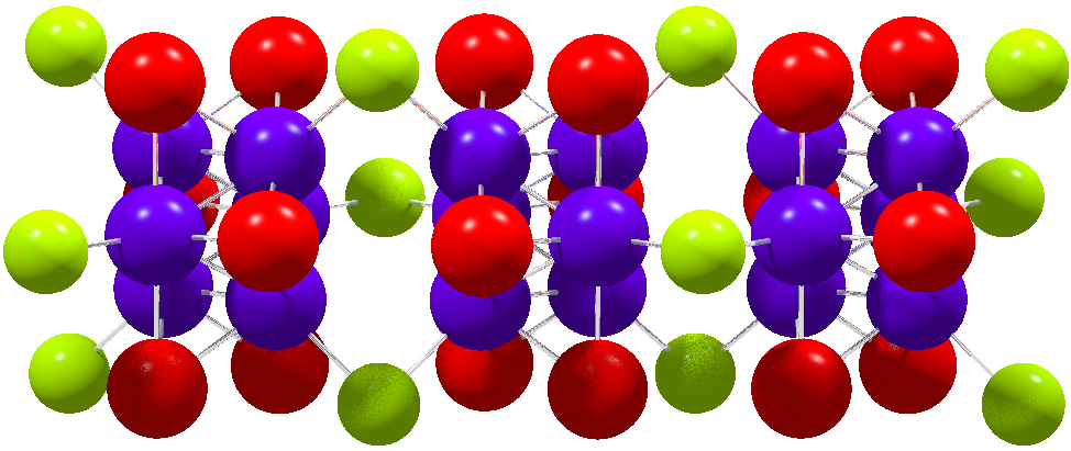
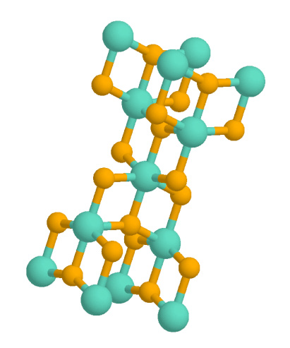
file:SnSe@SWCNT.jpg, upright=1.2, Crystalline 2×2-atom tin selenide nanowire grown inside a single-wall carbon nanotube (tube diameter ≈1 nm). A nanowire is a nanostructure in the form of a wire with the diameter of the order of a nanometre (10−9 m). More generally, nanowires can be defined as structures that have a thickness or diameter constrained to tens of nanometers or less and an unconstrained length. At these scales, quantum mechanical effects are important—which coined the term "quantum wires". Many different types of nanowires exist, including superconducting (e.g. Yttrium barium copper oxide, YBCO), metallic (e.g. nickel, Ni, platinum, Pt, gold, Au, silver, Ag), semiconducting (e.g. Silicon nanowire, silicon nanowires (SiNWs), indium phosphide, InP, gallium nitride, GaN) and insulating (e.g. Silicon dioxide, SiO2, Titanium dioxide, TiO2). Molecular nanowires are composed of repeating molecular units either organic (e.g. DNA) or inorganic (e.g. Mo6S9−''x'' ... [...More Info...] [...Related Items...] OR: [Wikipedia] [Google] [Baidu] |
Silicon Nanowire
Silicon nanowires, also referred to as SiNWs, are a type of semiconductor nanowire most often formed from a silicon precursor by etching of a solid or through catalyzed growth from a vapor or liquid phase. Such nanowires have promising applications in lithium-ion batteries, thermoelectrics and sensors. Initial synthesis of SiNWs is often accompanied by thermal oxidation steps to yield structures of accurately tailored size and morphology. SiNWs have unique properties that are not seen in bulk (three-dimensional) silicon materials. These properties arise from an unusual quasi one-dimensional electronic structure and are the subject of research across numerous disciplines and applications. The reason that SiNWs are considered one of the most important one-dimensional materials is they could have a function as building blocks for nanoscale electronics assembled without the need for complex and costly fabrication facilities. SiNWs are frequently studied towards applications including ph ... [...More Info...] [...Related Items...] OR: [Wikipedia] [Google] [Baidu] |
Molecular Nanowires
Molecular wires (or sometimes called molecular nanowires) are molecular chains that conduct electric current. They are the proposed building blocks for molecular electronic devices. Their typical diameters are less than three nanometers, while their lengths may be macroscopic, extending to centimeters or more. Examples Most types of molecular wires are derived from organic molecules. One naturally occurring molecular wire is DNA. Prominent inorganic examples include polymeric materials such as Li2Mo6Se6 and Mo6S9−xIx, d4(CO)4(OAc)4Pd(acac)2 and single-molecule extended metal atom chains (EMACs) which comprise strings of transition metal atoms directly bonded to each other. Molecular wires containing paramagnetic inorganic moieties can exhibit Kondo peaks. Conduction of electrons Molecular wires conduct electricity. They typically have non-linear current-voltage characteristics, and do not behave as simple ohmic conductors. The conductance follows typical power law behavio ... [...More Info...] [...Related Items...] OR: [Wikipedia] [Google] [Baidu] |
Gallium Nitride
Gallium nitride () is a binary III/ V direct bandgap semiconductor commonly used in blue light-emitting diodes since the 1990s. The compound is a very hard material that has a Wurtzite crystal structure. Its wide band gap of 3.4 eV affords it special properties for applications in optoelectronics, high-power and high-frequency devices. For example, GaN is the substrate that makes violet (405 nm) laser diodes possible, without requiring nonlinear optical frequency doubling. Its sensitivity to ionizing radiation is low (like other group III nitrides), making it a suitable material for solar cell arrays for satellites. Military and space applications could also benefit as devices have shown stability in high-radiation environments. Because GaN transistors can operate at much higher temperatures and work at much higher voltages than gallium arsenide (GaAs) transistors, they make ideal power amplifiers at microwave frequencies. In addition, GaN offers promising c ... [...More Info...] [...Related Items...] OR: [Wikipedia] [Google] [Baidu] |
Thermal Oxidation
In microfabrication, thermal oxidation is a way to produce a thin layer of oxide (usually silicon dioxide) on the surface of a wafer. The technique forces an oxidizing agent to diffuse into the wafer at high temperature and react with it. The rate of oxide growth is often predicted by the Deal–Grove model. Thermal oxidation may be applied to different materials, but most commonly involves the oxidation of silicon substrates to produce silicon dioxide. The chemical reaction Thermal oxidation of silicon is usually performed at a temperature between 800 and 1200 °C, resulting in a so-called High Temperature Oxide layer (HTO). It may use either water vapor (usually UHP steam) or molecular oxygen as the oxidant; it is consequently called either ''wet'' or ''dry'' oxidation. The reaction is one of the following: :\rm Si + 2H_2O \rightarrow SiO_2 + 2H_ :\rm Si + O_2 \rightarrow SiO_2 \, The oxidizing ambient may also contain several percent of hydrochloric acid (HCl). The chlo ... [...More Info...] [...Related Items...] OR: [Wikipedia] [Google] [Baidu] |
Quantum Wire
In mesoscopic physics, a quantum wire is an electrically conducting wire in which quantum effects influence the transport properties. Usually such effects appear in the dimension of nanometers, so they are also referred to as nanowires. Quantum effects If the diameter of a wire is sufficiently small, electrons will experience quantum confinement in the transverse direction. As a result, their transverse energy will be limited to a series of discrete values. One consequence of this quantization is that the classical formula for calculating the electrical resistance of a wire, : R = \rho \frac, is not valid for quantum wires (where \rho is the material's resistivity, l is the length, and A is the cross-sectional area of the wire). Instead, an exact calculation of the transverse energies of the confined electrons has to be performed to calculate a wire's resistance. Following from the quantization of electron energy, the electrical conductance (the inverse of the resistance) is fo ... [...More Info...] [...Related Items...] OR: [Wikipedia] [Google] [Baidu] |
Gold
Gold is a chemical element; it has chemical symbol Au (from Latin ) and atomic number 79. In its pure form, it is a brightness, bright, slightly orange-yellow, dense, soft, malleable, and ductile metal. Chemically, gold is a transition metal, a group 11 element, and one of the noble metals. It is one of the least reactivity (chemistry), reactive chemical elements, being the second-lowest in the reactivity series. It is solid under standard temperature and pressure, standard conditions. Gold often occurs in free elemental (native state (metallurgy), native state), as gold nugget, nuggets or grains, in rock (geology), rocks, vein (geology), veins, and alluvial deposits. It occurs in a solid solution series with the native element silver (as in electrum), naturally alloyed with other metals like copper and palladium, and mineral inclusions such as within pyrite. Less commonly, it occurs in minerals as gold compounds, often with tellurium (gold tellurides). Gold is resistant to ... [...More Info...] [...Related Items...] OR: [Wikipedia] [Google] [Baidu] |
Titanium Dioxide
Titanium dioxide, also known as titanium(IV) oxide or titania , is the inorganic compound derived from titanium with the chemical formula . When used as a pigment, it is called titanium white, Pigment White 6 (PW6), or Colour Index International, CI 77891. It is a white solid that is insoluble in water, although mineral forms can appear black. As a pigment, it has a wide range of applications, including paint, sunscreen, and food coloring. When used as a food coloring, it has E number E171. World production in 2014 exceeded 9 million tonnes. It has been estimated that titanium dioxide is used in two-thirds of all pigments, and pigments based on the oxide have been valued at a price of $13.2 billion. Structure In all three of its main dioxides, titanium exhibits Octahedral molecular geometry, octahedral geometry, being bonded to six oxide anions. The oxides in turn are bonded to three Ti centers. The overall crystal structures of rutile and anatase are tetragonal in symmetry ... [...More Info...] [...Related Items...] OR: [Wikipedia] [Google] [Baidu] |
Quantum Of Conductance
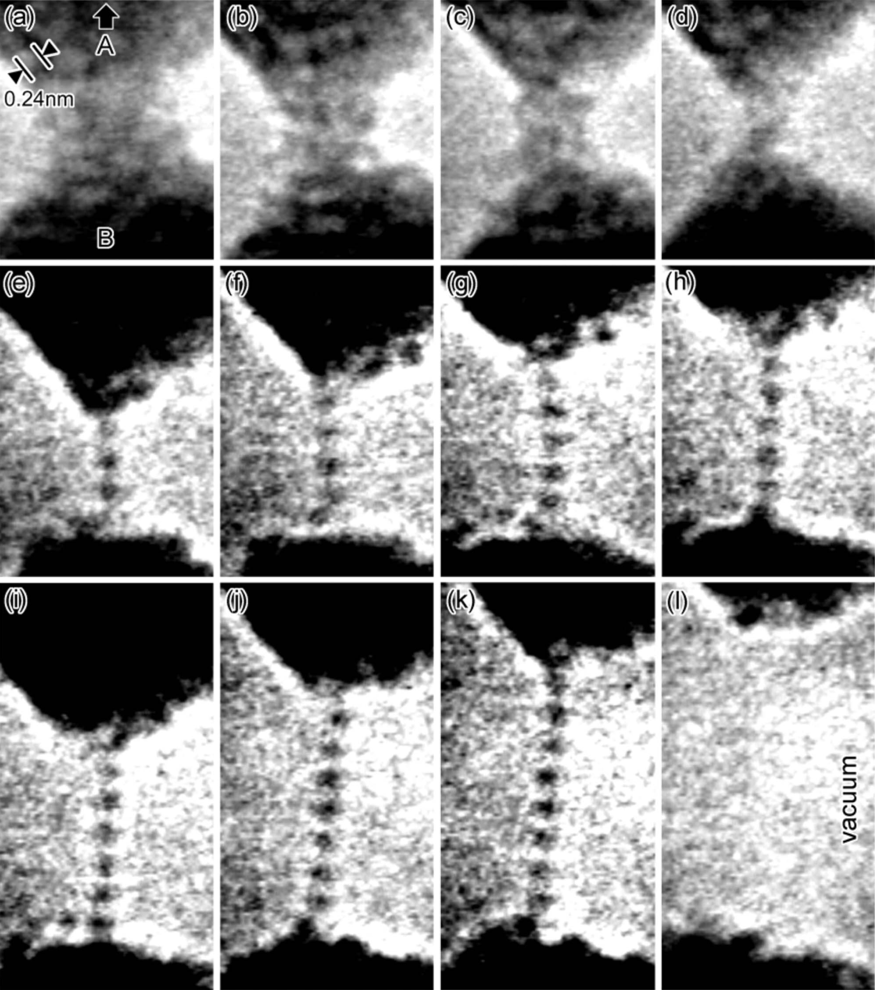
The conductance quantum, denoted by the symbol , is the quantized unit of electrical conductance. It is defined by the elementary charge ''e'' and Planck constant ''h'' as: : G_0 = \frac = 4 \alpha \epsilon_0 c = It appears when measuring the conductance of a quantum point contact, and, more generally, is a key component of the Landauer formula, which relates the electrical conductance of a quantum conductor to its quantum properties. It is twice the reciprocal of the von Klitzing constant (2/''R''K). Note that the conductance quantum does not mean that the conductance of any system must be an integer multiple of ''G''0. Instead, it describes the conductance of two quantum channels (one channel for spin up and one channel for spin down) if the probability for transmitting an electron that enters the channel is unity, i.e. if transport through the channel is ballistic. If the transmission probability is less than unity, then the conductance of the channel is less than ''G''0. T ... [...More Info...] [...Related Items...] OR: [Wikipedia] [Google] [Baidu] |
Von Klitzing Constant
The quantum Hall effect (or integer quantum Hall effect) is a quantized version of the Hall effect which is observed in two-dimensional electron systems subjected to low temperatures and strong magnetic fields, in which the Hall resistance exhibits steps that take on the quantized values : R_ = \frac = \frac , where is the Hall voltage, is the channel current, is the elementary charge and is the Planck constant. The divisor can take on either integer () or fractional () values. Here, is roughly but not exactly equal to the filling factor of Landau levels. The quantum Hall effect is referred to as the integer or fractional quantum Hall effect depending on whether is an integer or fraction, respectively. The striking feature of the integer quantum Hall effect is the persistence of the quantization (i.e. the Hall plateau) as the electron density is varied. Since the electron density remains constant when the Fermi level is in a clean spectral gap, this situation corres ... [...More Info...] [...Related Items...] OR: [Wikipedia] [Google] [Baidu] |


