|
Acer Laboratories Incorporated
ALi Corporation (also known as Acer Laboratories Incorporated or Acer Labs Inc., and commonly known as ALi) is a major designer and manufacturer of embedded systems integrated circuits, and a former manufacturer of personal computer integrated circuits. It is based in Taiwan, and is a subsidiary of the Acer group. The company was founded in 1987, its president is Teddy Lu. Part of ALi including the personal computer integrated circuits business was spun off as ULi Electronics Inc. in June 2003. ULi was acquired by Nvidia in 2006 for $52 million. Products Chipsets 80X86 Chipsets Pentium and Socket 7 Chipsets Slot 1 and Socket 370 Chipsets Slot A and Socket A Chipsets Socket 478 Chipsets Socket 754/939/940 Chipsets Southbridge Chips Image:Gigabyte GA-5AX rev. 3.0 20081118.jpg, ALi M1541-based motherboard with AMD K6-2 300MHz processor. Image:Ali M1535.jpg, ALi M1535 southbridge chip from a Fujitsu Lifebook P series laptop VGA * M3141 * M3143 * M3145A Al ... [...More Info...] [...Related Items...] OR: [Wikipedia] [Google] [Baidu] |
Semiconductor Industry
The semiconductor industry is the aggregate of companies engaged in the design and fabrication of semiconductors and semiconductor devices, such as transistors and integrated circuits. It formed around 1960, once the fabrication of semiconductor devices became a viable business. The industry's annual semiconductor sales revenue has since grown to over , as of 2018. The semiconductor industry is in turn the driving force behind the wider electronics industry, with annual power electronics sales of £135billion () as of 2011, annual consumer electronics sales expected to reach by 2020, tech industry sales expected to reach in 2019, and e-commerce with over in 2017. In 2019, 32.4% of the semiconductor market segment was for networks and communications devices. In 2021, the sales of semiconductors reached a record $555.9 billion, up 26.2 percent with sales in China reaching $192.5 billion, according to the Semiconductor Industry Association. A record 1.15 trillion semicondu ... [...More Info...] [...Related Items...] OR: [Wikipedia] [Google] [Baidu] |
VESA Local Bus
The VESA Local Bus (usually abbreviated to VL-Bus or VLB) is a short-lived expansion bus introduced during the i486 generation of x86 IBM-compatible personal computers. Created by VESA (Video Electronics Standards Association), the VESA Local Bus worked alongside the then-dominant ISA bus to provide a standardized high-speed conduit intended primarily to accelerate video (graphics) operations. VLB provides a standardized fast path that add-in (video) card makers could tap for greatly accelerated memory-mapped I/O and DMA, while still using the familiar ISA bus to handle basic device duties such as interrupts and port-mapped I/O. Some high-end 386dx motherboards also had a VL-Bus slot. Historical overview In the early 1990s, the I/O bandwidth of the prevailing ISA bus, 8.33 MB/s for standard 16 bit 8.33 MHz slots, had become a critical bottleneck to PC video and graphics performance. The need for faster graphics was driven by increased adoption of graphical user interf ... [...More Info...] [...Related Items...] OR: [Wikipedia] [Google] [Baidu] |
Pentium III
The Pentium III (marketed as Intel Pentium III Processor, informally PIII or P3) brand refers to Intel's 32-bit x86 desktop and mobile CPUs based on the sixth-generation P6 microarchitecture introduced on February 28, 1999. The brand's initial processors were very similar to the earlier Pentium II-branded processors. The most notable differences were the addition of the Streaming SIMD Extensions (SSE) instruction set (to accelerate floating point and parallel calculations), and the introduction of a controversial serial number embedded in the chip during manufacturing. The Pentium III is also a single-core processor. Even after the release of the Pentium 4 in late 2000, the Pentium III continued to be produced with new models introduced until early 2003, and were discontinued in April 2004 for desktop units, and May 2007 for mobile units. Processor cores Similarly to the Pentium II it superseded, the Pentium III was also accompanied by the Celeron brand for lower-end ver ... [...More Info...] [...Related Items...] OR: [Wikipedia] [Google] [Baidu] |
Pentium II
The Pentium II brand refers to Intel's sixth-generation microarchitecture (" P6") and x86-compatible microprocessors introduced on May 7, 1997. Containing 7.5 million transistors (27.4 million in the case of the mobile Dixon with 256 KB L2 cache), the Pentium II featured an improved version of the first ''P6''-generation core of the Pentium Pro, which contained 5.5 million transistors. However, its L2 cache subsystem was a downgrade when compared to the Pentium Pros. It is a single-core microprocessor. In 1998, Intel stratified the Pentium II family by releasing the Pentium II-based Celeron line of processors for low-end workstations and the Pentium II Xeon line for servers and high-end workstations. The Celeron was characterized by a reduced or omitted (in some cases present but disabled) on-die full-speed L2 cache and a 66 MT/s FSB. The Xeon was characterized by a range of full-speed L2 cache (from 512 KB to 2048 KB), a 100 MT/s FSB, a different phys ... [...More Info...] [...Related Items...] OR: [Wikipedia] [Google] [Baidu] |
Socket 370
Socket 370 (also known as the PGA370 socket) is a CPU socket first used by Intel for Pentium III and Celeron processors to first complement and later replace the older Slot 1 CPU interface on personal computers. The "370" refers to the number of pin holes in the socket for CPU pins. Socket 370 was replaced by Socket 423 in 2000. Overview Socket 370 started as a budget oriented platform for 66 MHz FSB PPGA Mendocino Celeron CPUs in late 1998, as the move to on-die L2 cache removed the need for a PCB design as seen on Slot 1. From late 1999 to late 2000 it was Intel's main desktop socket for 100/133 MHz FSB Coppermine Pentium IIIs. In 2001, the Tualatin Pentium III processors brought changes to the infrastructure which required dedicated Tualatin-compatible motherboards; some manufacturers would indicate this with a blue (instead of white) socket. These late sockets were typically compatible with Coppermine processors, but not older Mendocino Celerons. Some motherboards that ... [...More Info...] [...Related Items...] OR: [Wikipedia] [Google] [Baidu] |
Slot 1
Slot 1 refers to the physical and electrical specification for the connector used by some of Intel's microprocessors, including the Pentium Pro, Celeron, Pentium II and the Pentium III. Both single and dual processor configurations were implemented. Intel reverted to the traditional socket interface with Socket 370 in 1999. General With the introduction of the Pentium II CPU, the need for greater access for testing had made the transition from socket to slot necessary. Previously with the Pentium Pro, Intel had combined processor and cache dies in the same Socket 8 package. These were connected by a full-speed bus, resulting in significant performance benefits. Unfortunately, this method required that the two components be bonded together early in the production process, before testing was possible. As a result, a single, tiny flaw in either die made it necessary to discard the entire assembly, causing low production yield and high cost. Intel subsequently designed a ci ... [...More Info...] [...Related Items...] OR: [Wikipedia] [Google] [Baidu] |
Super Socket 7
Super Socket 7, also referred to as Super 7, is a hardware-level extension of the Socket 7 ZIF socket specification for x86 processors. Compatible motherboards and chipsets use a standard Socket 7 connection for the CPU, while adding certain features including a maximum 100 MHz front-side bus and support for AGP graphics cards. Super Socket 7 was used by AMD K6-2 and K6-III processors, some of the final Cyrix M-II processors, some of the final IDT WinChip 2 processors, and Rise mP6 processors. It is backward compatible with Socket 7 CPUs, meaning a Socket 7 CPU can be used with a Super Socket 7 motherboard, but a Super Socket 7 CPU cannot operate at full speed in a Socket 7 motherboard. Socket 5 CPUs are pin-compatible with Super Socket 7, but not all motherboards designed for Super Socket 7 supported the voltages or bus speeds needed for Socket 5 CPUs. While AMD had previously always used Intel sockets for their processors, Socket 7 was the last one for which AMD ret ... [...More Info...] [...Related Items...] OR: [Wikipedia] [Google] [Baidu] |
SDRAM
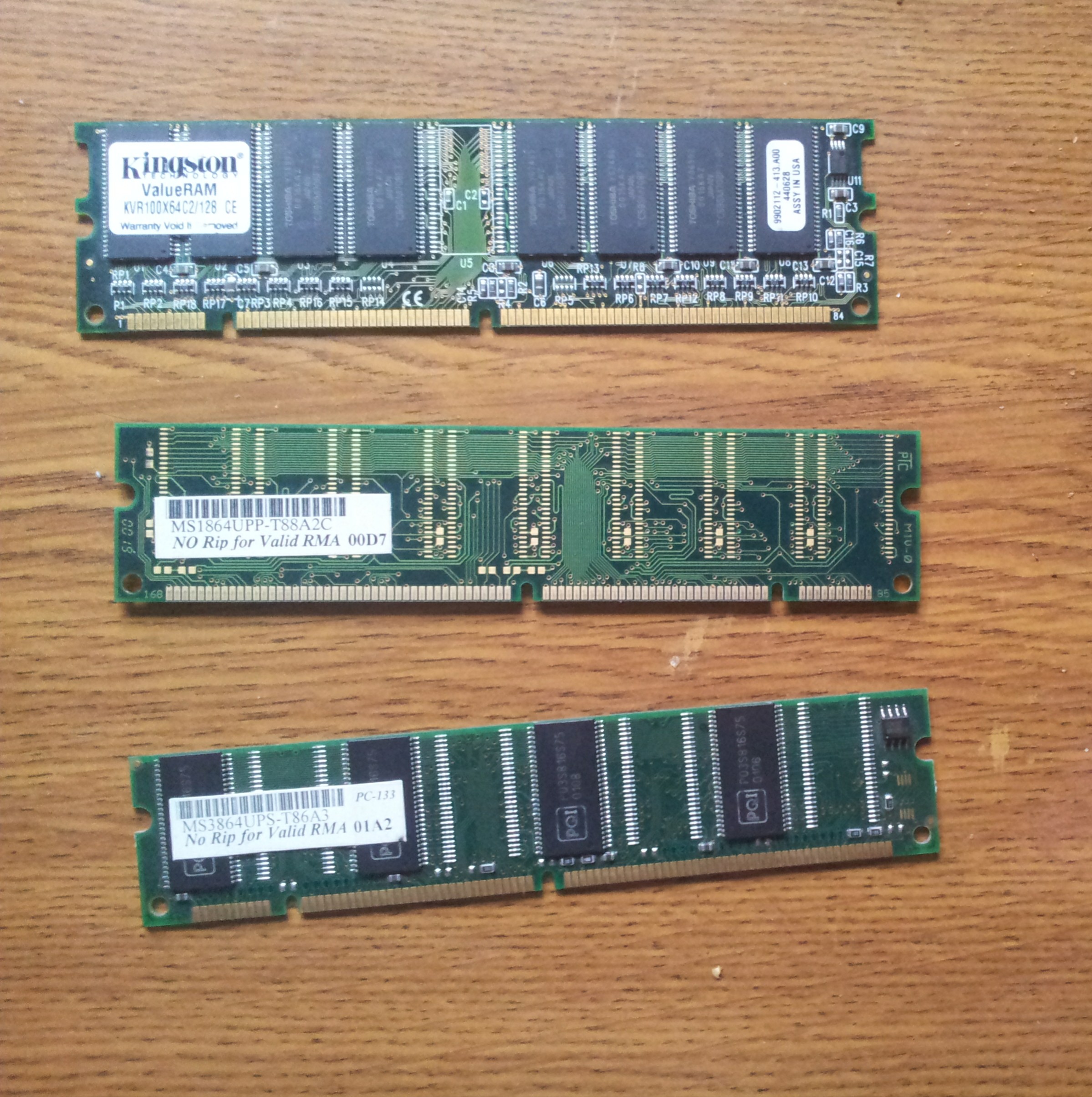
Synchronous dynamic random-access memory (synchronous dynamic RAM or SDRAM) is any DRAM where the operation of its external pin interface is coordinated by an externally supplied clock signal. DRAM integrated circuits (ICs) produced from the early 1970s to early 1990s used an ''asynchronous'' interface, in which input control signals have a direct effect on internal functions only delayed by the trip across its semiconductor pathways. SDRAM has a ''synchronous'' interface, whereby changes on control inputs are recognised after a rising edge of its clock input. In SDRAM families standardized by JEDEC, the clock signal controls the stepping of an internal finite-state machine that responds to incoming commands. These commands can be pipelined to improve performance, with previously started operations completing while new commands are received. The memory is divided into several equally sized but independent sections called '' banks'', allowing the device to operate on a memor ... [...More Info...] [...Related Items...] OR: [Wikipedia] [Google] [Baidu] |
Socket 7
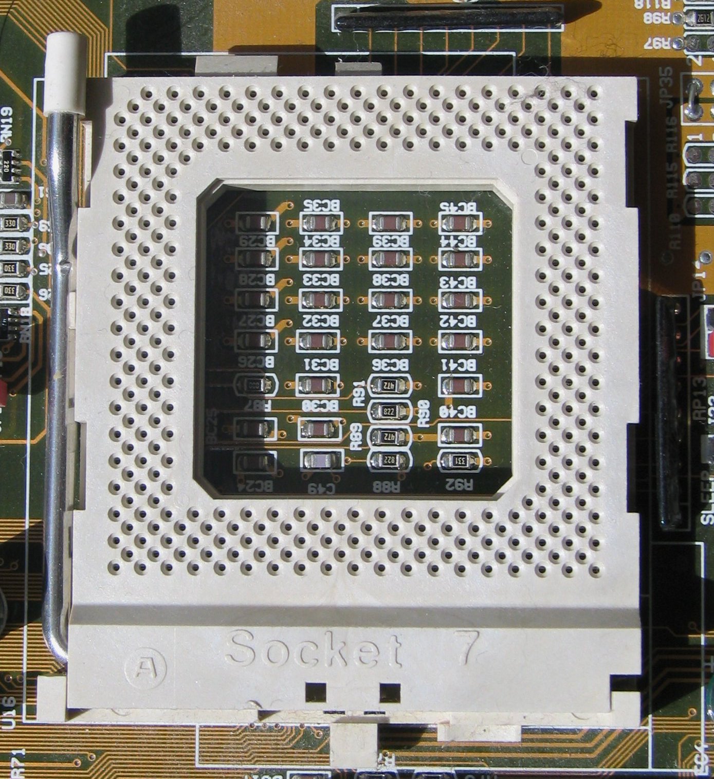
Socket 7 is a physical and electrical specification for an x86-style CPU socket on a personal computer motherboard. It was released in June 1995. The socket supersedes the earlier Socket 5, and accepts P5 Pentium microprocessors manufactured by Intel, as well as compatibles made by Cyrix/ IBM, AMD, IDT and others. Socket 7 was the only socket that supported a wide range of CPUs from different manufacturers and a wide range of speeds. Differences between Socket 5 and Socket 7 are that Socket 7 has an extra pin and is designed to provide dual split rail voltage, as opposed to Socket 5's single voltage. However, not all motherboard manufacturers supported the dual voltage on their boards initially. Socket 7 is backwards compatible; a Socket 5 CPU can be inserted and used on a Socket 7 motherboard. Processors that used Socket 7 are the AMD K5 and K6, the Cyrix 6x86 and 6x86MX, the IDT WinChip, the Intel P5 Pentium (2.5–3.5 V, 75–200 MHz), the Pentium MMX (166–23 ... [...More Info...] [...Related Items...] OR: [Wikipedia] [Google] [Baidu] |
Socket 5
Socket 5 was created for the second generation of Intel P5 Pentium processors operating at speeds from 75 to 133 MHz as well as certain Pentium OverDrive and Pentium MMX processors with core voltage 3.3 V. It superseded the earlier Socket 4. It was released in March 1994. Consisting of 320 pins, this was the first socket to use a staggered pin grid array, or SPGA, which allowed the chip's pins to be spaced closer together than earlier sockets. Socket 5 was replaced by Socket 7 in 1995. External linksDifferences between Socket 5 and Socket 7(archived) See also * List of Intel microprocessors * List of AMD microprocessors This article gives a list of AMD microprocessors, sorted by generation and release year. If applicable and openly known, the designation(s) of each processor's core (versions) is (are) listed in parentheses. For an overview over concrete product, ... References {{earlysock Socket 005 ... [...More Info...] [...Related Items...] OR: [Wikipedia] [Google] [Baidu] |
Socket 4
Socket 4, presented in 1993, was the first CPU socket designed for the early P5 Pentium microprocessors. Socket 4 was the only 5-volt socket for the Pentium. Socket 4 does support a special Pentium OverDrive, which allows running at 120 MHz (for the 60 MHz Pentium) or 133 MHz (for the 66 MHz Pentium). Socket 4 was superseded by the 3.3-volt-powered Socket 5 in 1994. See also * List of Intel microprocessors This generational list of Intel processors attempts to present all of Intel's processors from the pioneering 4-bit 4004 (1971) to the present high-end offerings. Concise technical data is given for each product. Latest 13th generation Cor ... References {{earlysock Socket 004 ... [...More Info...] [...Related Items...] OR: [Wikipedia] [Google] [Baidu] |
Accelerated Graphics Port
Accelerated Graphics Port (AGP) is a parallel expansion card standard, designed for attaching a video card to a computer system to assist in the acceleration of 3D computer graphics. It was originally designed as a successor to PCI-type connections for video cards. Since 2004, AGP was progressively phased out in favor of PCI Express (PCIe), which is serial, as opposed to parallel; by mid-2008, PCI Express cards dominated the market and only a few AGP models were available, with GPU manufacturers and add-in board partners eventually dropping support for the interface in favor of PCI Express. Advantages over PCI AGP is a superset of the PCI standard, designed to overcome PCI's limitations in serving the requirements of the era's high-performance graphics cards. The primary advantage of AGP is that it doesn't share the PCI bus, providing a dedicated, point-to-point pathway between the expansion slot(s) and the motherboard chipset. The direct connection also allows for higher cl ... [...More Info...] [...Related Items...] OR: [Wikipedia] [Google] [Baidu] |


