|
Vortex86
The Vortex86 is a computing system-on-a-chip (SoC) based on a core compatible with the x86 microprocessor family. It is produced by DM&P Electronics, but originated with Rise Technology. History Vortex86 previously belonged to SiS, which got the basic design from Rise Technology. SiS sold it to DM&P Electronics in Taiwan. Before adopting the Vortex86 series, DM&P manufactured the ALi M6117D, which contains VM Technology VMT386SX+ derived x86 core, an Intel 386SX compatible, 25–40 MHz SoC. CPU Vortex86 CPUs implement the IA-32 architecture but which instructions are implemented varies depending on the model. Vortex86SX and the early versions of Vortex86 do not have a floating point unit (FPU). Any code that runs on i586 but does not use floating point instructions will run on these models. Any i586 code will run on Vortex86DX and later. Some Linux kernels (by build-time option) emulate the FPU on any CPU that is missing one, so a program that uses i586-level floating ... [...More Info...] [...Related Items...] OR: [Wikipedia] [Google] [Baidu] |
Windows IoT
Windows IoT, short for Windows Internet of Things and formerly known as Windows Embedded, is a family of operating systems from Microsoft designed for use in embedded systems. Microsoft has three different subfamilies of operating systems for embedded devices targeting a wide market, ranging from small-footprint, real-time devices to point of sale (POS) devices like kiosks. Windows Embedded operating systems are available to original equipment manufacturers (OEMs), who make it available to end users preloaded with their hardware, in addition to volume license customers in some cases. In April 2018, Microsoft released Azure Sphere, another operating system designed for IoT applications running on the Linux kernel. The IoT family Microsoft rebranded "Windows Embedded" to "Windows IoT" starting with the release of embedded editions of Windows 10. Enterprise Windows IoT Enterprise is a binary equivalent version of Windows 10 and 11 Enterprise designed for use in embedded appli ... [...More Info...] [...Related Items...] OR: [Wikipedia] [Google] [Baidu] |
Industry Standard Architecture
Industry Standard Architecture (ISA) is the 16-bit internal bus (computing), bus of IBM PC/AT and similar computers based on the Intel 80286 and its immediate successors during the 1980s. The bus was (largely) backward compatible with the 8-bit bus of the 8088-based IBM PC, including the IBM PC/XT as well as IBM PC compatibles. Originally referred to as the PC bus (8-bit) or AT bus (16-bit), it was also termed ''I/O Channel'' by IBM. The ISA term was coined as a retronym by IBM PC clone manufacturers in the late 1980s or early 1990s as a reaction to IBM attempts to replace the AT bus with its new and incompatible Micro Channel architecture. The 16-bit ISA bus was also used with 32-bit processors for several years. An attempt to extend it to 32 bits, called Extended Industry Standard Architecture (EISA), was not very successful, however. Later buses such as VESA Local Bus and Peripheral Component Interconnect, PCI were used instead, often along with ISA slots on the same mainbo ... [...More Info...] [...Related Items...] OR: [Wikipedia] [Google] [Baidu] |
Peripheral Component Interconnect
Peripheral Component Interconnect (PCI) is a local computer bus for attaching hardware devices in a computer and is part of the PCI Local Bus standard. The PCI bus supports the functions found on a processor bus but in a standardized format that is independent of any given processor's native bus. Devices connected to the PCI bus appear to a bus master to be connected directly to its own bus and are assigned addresses in the processor's address space. It is a parallel bus, synchronous to a single bus clock. Attached devices can take either the form of an integrated circuit fitted onto the motherboard (called a ''planar device'' in the PCI specification) or an expansion card that fits into a slot. The PCI Local Bus was first implemented in IBM PC compatibles, where it displaced the combination of several slow Industry Standard Architecture (ISA) slots and one fast VESA Local Bus (VLB) slot as the bus configuration. It has subsequently been adopted for other computer types ... [...More Info...] [...Related Items...] OR: [Wikipedia] [Google] [Baidu] |
DDR2 SDRAM
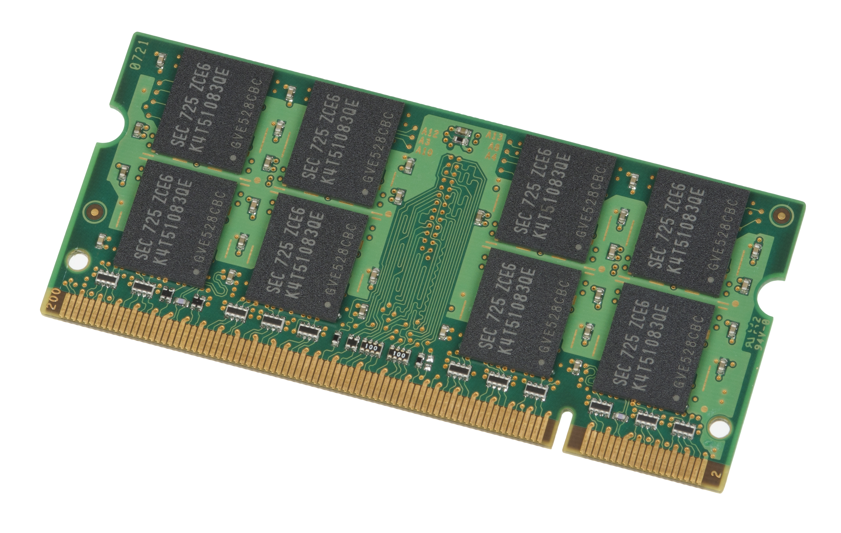
Double Data Rate 2 Synchronous Dynamic Random-Access Memory (DDR2 SDRAM) is a double data rate (DDR) synchronous dynamic random-access memory (SDRAM) interface. It is a JEDEC standard (JESD79-2); first published in September 2003. DDR2 succeeded the original DDR SDRAM specification, and was itself succeeded by DDR3 SDRAM in 2007. DDR2 DIMMs are neither forward compatible with DDR3 nor backward compatible with DDR. In addition to double pumping the data bus as in DDR SDRAM (transferring data on the rising and falling edges of the bus clock signal), DDR2 allows higher bus speed and requires lower power by running the internal clock at half the speed of the data bus. The two factors combine to produce a total of four data transfers per internal clock cycle. Since the DDR2 internal clock runs at half the DDR external clock rate, DDR2 memory operating at the same external data bus clock rate as DDR results in DDR2 being able to provide the same bandwidth but with better la ... [...More Info...] [...Related Items...] OR: [Wikipedia] [Google] [Baidu] |
SDRAM
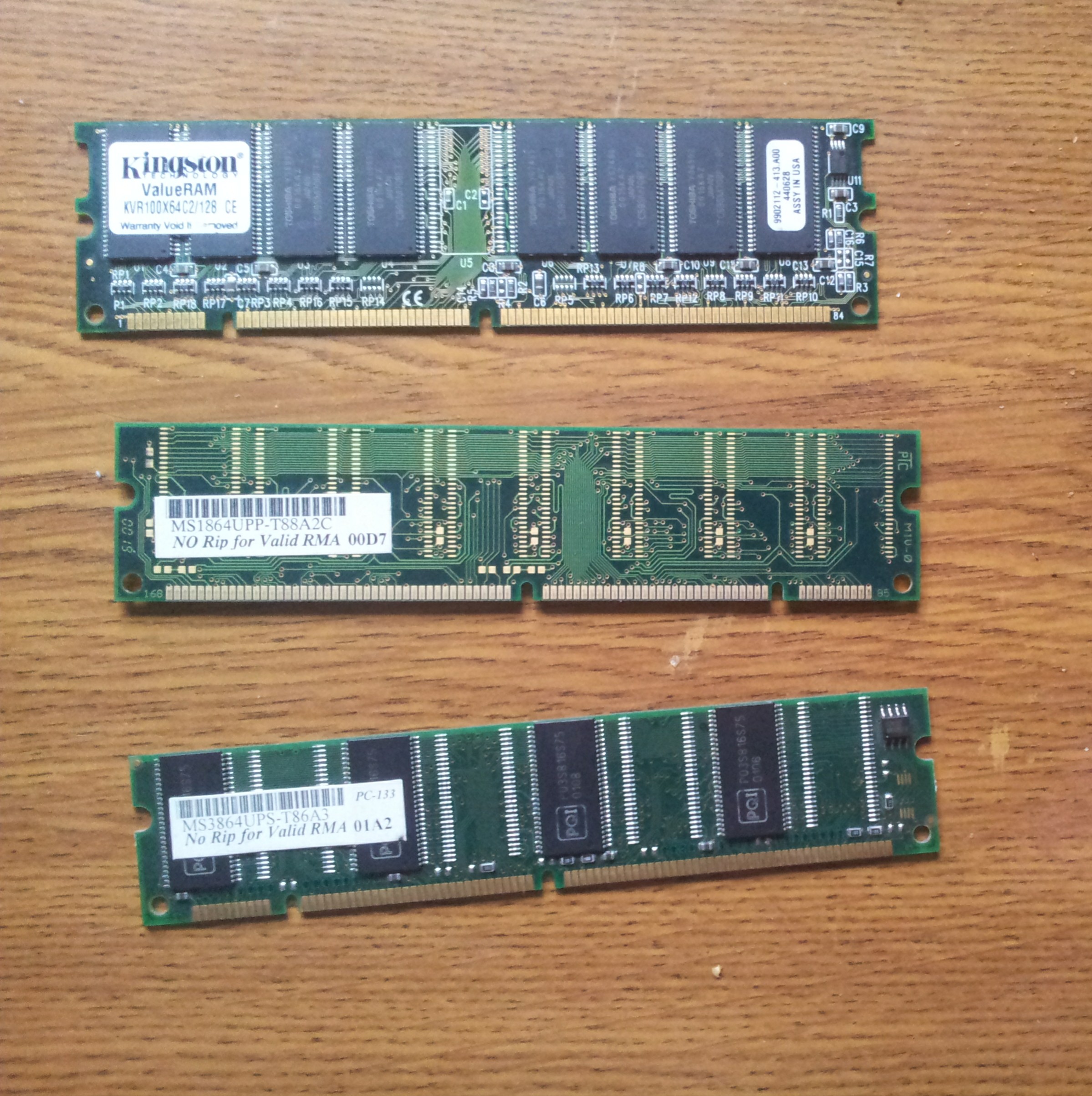
Synchronous dynamic random-access memory (synchronous dynamic RAM or SDRAM) is any DRAM where the operation of its external pin interface is coordinated by an externally supplied clock signal. DRAM integrated circuits (ICs) produced from the early 1970s to the early 1990s used an ''asynchronous'' interface, in which input control signals have a direct effect on internal functions delayed only by the trip across its semiconductor pathways. SDRAM has a ''synchronous'' interface, whereby changes on control inputs are recognised after a rising edge of its clock input. In SDRAM families standardized by JEDEC, the clock signal controls the stepping of an internal finite-state machine that responds to incoming commands. These commands can be pipelined to improve performance, with previously started operations completing while new commands are received. The memory is divided into several equally sized but independent sections called ''banks'', allowing the device to operate on a memor ... [...More Info...] [...Related Items...] OR: [Wikipedia] [Google] [Baidu] |
Floating-point Unit
A floating-point unit (FPU), numeric processing unit (NPU), colloquially math coprocessor, is a part of a computer system specially designed to carry out operations on floating-point numbers. Typical operations are addition, subtraction, multiplication, division, and square root. Modern designs generally include a fused multiply-add instruction, which was found to be very common in real-world code. Some FPUs can also perform various transcendental functions such as exponential or trigonometric calculations, but the accuracy can be low, so some systems prefer to compute these functions in software. Floating-point operations were originally handled in software in early computers. Over time, manufacturers began to provide standardized floating-point libraries as part of their software collections. Some machines, those dedicated to scientific processing, would include specialized hardware to perform some of these tasks with much greater speed. The introduction of microcode in ... [...More Info...] [...Related Items...] OR: [Wikipedia] [Google] [Baidu] |
CPU Cache
A CPU cache is a hardware cache used by the central processing unit (CPU) of a computer to reduce the average cost (time or energy) to access data from the main memory. A cache is a smaller, faster memory, located closer to a processor core, which stores copies of the data from frequently used main memory locations. Most CPUs have a hierarchy of multiple cache levels (L1, L2, often L3, and rarely even L4), with different instruction-specific and data-specific caches at level 1. The cache memory is typically implemented with static random-access memory (SRAM), in modern CPUs by far the largest part of them by chip area, but SRAM is not always used for all levels (of I- or D-cache), or even any level, sometimes some latter or all levels are implemented with eDRAM. Other types of caches exist (that are not counted towards the "cache size" of the most important caches mentioned above), such as the translation lookaside buffer (TLB) which is part of the memory management unit (M ... [...More Info...] [...Related Items...] OR: [Wikipedia] [Google] [Baidu] |
Cache (computing)
In computing, a cache ( ) is a hardware or software component that stores data so that future requests for that data can be served faster; the data stored in a cache might be the result of an earlier computation or a copy of data stored elsewhere. A cache hit occurs when the requested data can be found in a cache, while a cache miss occurs when it cannot. Cache hits are served by reading data from the cache, which is faster than recomputing a result or reading from a slower data store; thus, the more requests that can be served from the cache, the faster the system performs. To be cost-effective, caches must be relatively small. Nevertheless, caches are effective in many areas of computing because typical Application software, computer applications access data with a high degree of locality of reference. Such access patterns exhibit temporal locality, where data is requested that has been recently requested, and spatial locality, where data is requested that is stored near dat ... [...More Info...] [...Related Items...] OR: [Wikipedia] [Google] [Baidu] |
Cache Placement Policies
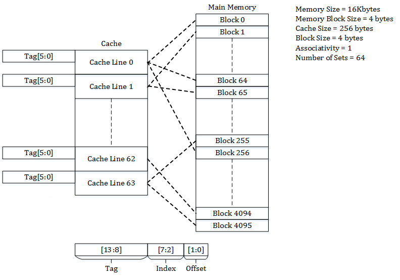
Cache placement policies are policies that determine where a particular memory block can be placed when it goes into a CPU cache. A block of memory cannot necessarily be placed at an arbitrary location in the cache; it may be restricted to a particular cache line or a set of cache lines by the cache's placement policy. There are three different policies available for placement of a memory block in the cache: direct-mapped, fully associative, and set-associative. Originally this space of cache organizations was described using the term "congruence mapping". Direct-mapped cache In a direct-mapped cache structure, the cache is organized into multiple sets with a single cache line per set. Based on the address of the memory block, it can only occupy a single cache line. The cache can be framed as a column matrix. To place a block in the cache * The set is determined by the index bits derived from the address of the memory block. * The memory block is placed in the set identif ... [...More Info...] [...Related Items...] OR: [Wikipedia] [Google] [Baidu] |
I486SX
The i486SX was a microprocessor originally released by Intel in 1991. It was a modified Intel i486, i486DX microprocessor with its Floating-point unit, floating-point unit (FPU) disabled. It was intended as a lower-cost CPU for use in low-end systems—selling for United States dollar, US$258—adapting the ''SX'' suffix of the earlier i386SX in order to connote a lower-cost option. However, unlike the i386SX, which had a 16-bit external data bus and a 24-bit external address bus (compared to the fully 32-bit i386DX, its higher-cost counterpoint), the i486SX was entirely 32-bit. The Intel486 SX-20 CPU can perform up 20 MIPS at 25 MHertz, Hz while this can also perform 70% faster than the 33 MHz Intel386 DX with external cache. Overview In the early 1990s, common applications, such as word processors and database applications, did not need or benefit from a floating-point unit, such as that included in the i486, introduced in 1989. Among the rare exceptions were Computer-aided desi ... [...More Info...] [...Related Items...] OR: [Wikipedia] [Google] [Baidu] |
Ball Grid Array
A ball grid array (BGA) is a type of surface-mount packaging (a chip carrier) used for integrated circuits. BGA packages are used to permanently mount devices such as microprocessors. A BGA can provide more interconnection pins than can be put on a dual in-line or flat package. The whole bottom surface of the device can be used, instead of just the perimeter. The traces connecting the package's leads to the wires or balls which connect the die to package are also on average shorter than with a perimeter-only type, leading to better performance at high speeds. Soldering of BGA devices requires precise control and is usually done by automated processes such as in computer-controlled automatic reflow ovens. Description The BGA is descended from the pin grid array (PGA), which is a package with one face covered (or partly covered) with pins in a grid pattern which, in operation, conduct electrical signals between the integrated circuit and the printed circuit board (PCB) ... [...More Info...] [...Related Items...] OR: [Wikipedia] [Google] [Baidu] |


