|
Substrate Mapping
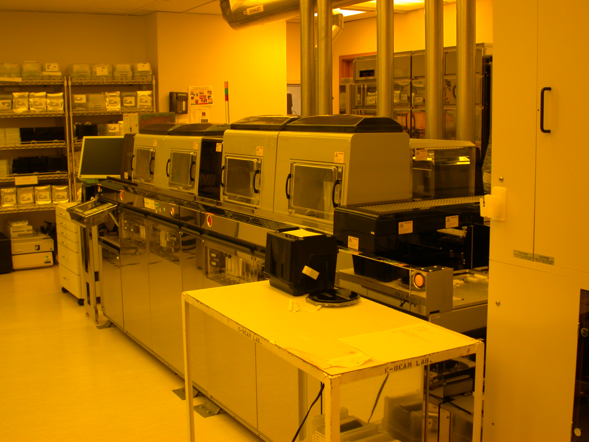
Substrate mapping (or wafer mapping) is a process in which the performance of semiconductor device fabrication, semiconductor devices on a substrate is represented by a map showing the performance as a colour-coded grid. The map is a convenient representation of the variation in performance across the substrate, since the distribution of those variations may be a clue as to their cause. The concept also includes the package of data generated by modern wafer testing equipment which can be transmitted to equipment used for subsequent 'back-end' manufacturing operations. History The initial process supported by substrate maps was inkless binning. Each tested die is assigned a bin value, depending on the result of the test. For example, a pass die is assigned a bin value of 1 for a good bin, bin 10 for an open circuit, and bin 11 for a short circuit. In the very early days of wafer test, the dies were put in different bins or buckets, depending on the test results. Physical binning ... [...More Info...] [...Related Items...] OR: [Wikipedia] [Google] [Baidu] |
|
 |
Semiconductor Device Fabrication
Semiconductor device fabrication is the process used to manufacture semiconductor devices, typically integrated circuits (ICs) such as microprocessors, microcontrollers, and memories (such as Random-access memory, RAM and flash memory). It is a multiple-step Photolithography, photolithographic and physico-chemical process (with steps such as thermal oxidation, thin-film deposition, ion-implantation, etching) during which electronic circuits are gradually created on a wafer (electronics), wafer, typically made of pure single-crystal semiconducting material. Silicon is almost always used, but various compound semiconductors are used for specialized applications. This article focuses on the manufacture of integrated circuits, however steps such as etching and photolithography can be used to manufacture other devices such as LCD and OLED displays. The fabrication process is performed in highly specialized semiconductor fabrication plants, also called foundries or "fabs", with the cen ... [...More Info...] [...Related Items...] OR: [Wikipedia] [Google] [Baidu] |
 |
Wafer Testing
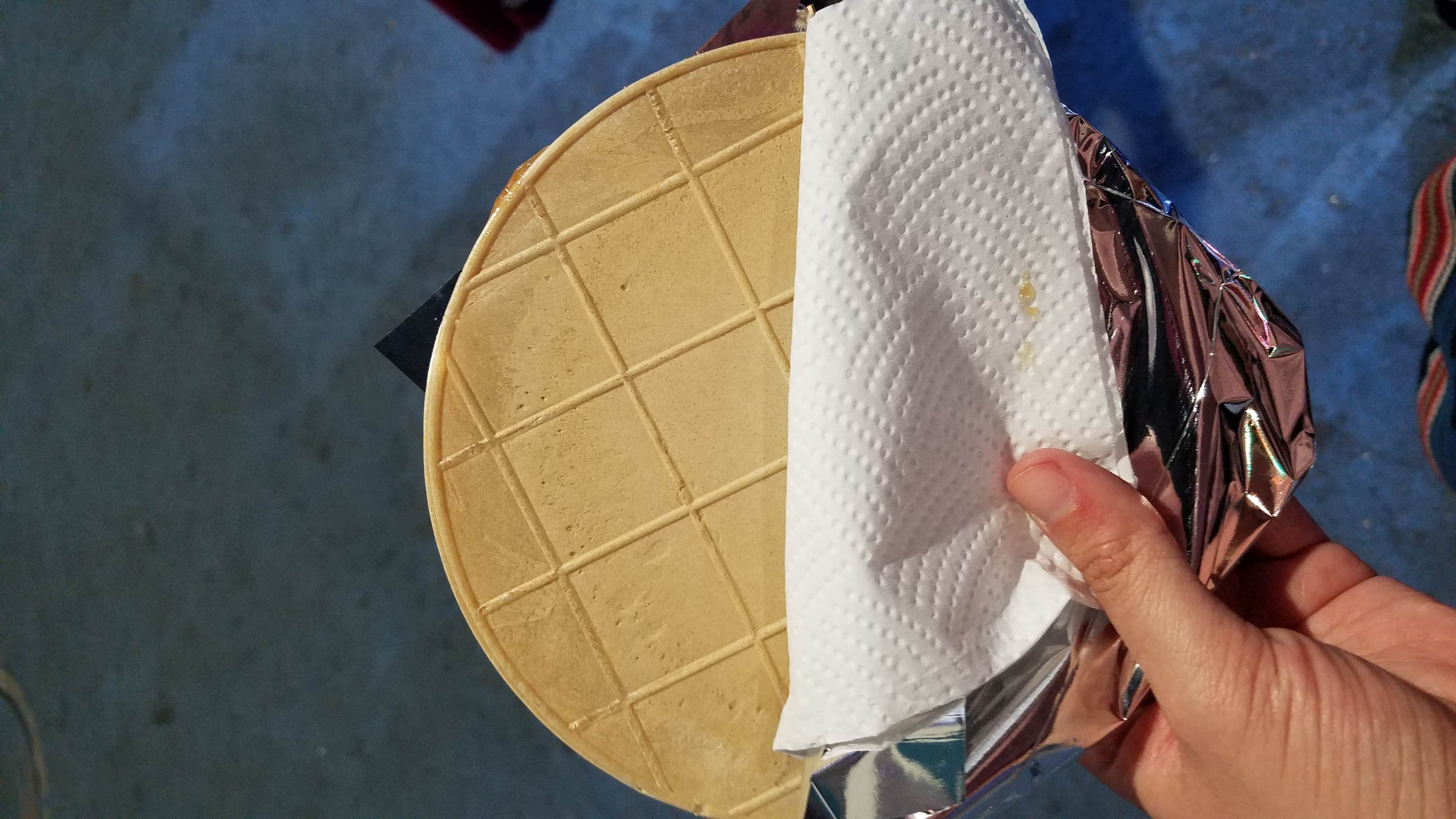
A wafer is a crisp, often sweet, very thin, flat, light biscuit, often used to decorate ice cream, and also used as a Garnish (food), garnish on some sweet dishes. They frequently have a waffle surface pattern but may also be patterned with insignia of the food's manufacturer or may be patternless. Some chocolate bars, such as Kit Kat and Toffee Crisp, are wafers with chocolate in and around them. Communion wafers A communion wafer is a type of unleavened bread consumed as part of the Christian ritual of communion. Spa wafer Special "spa wafers" (Czech: ''lázeňské oplatky'', Slovak: ''kúpeľné oblátky'') are produced in the spa towns of the Czech Republic and the Slovak Republic (e.g. Piešťany). The production of the wafers in Karlovy Vary, Karlsbad and Mariánské Lázně, Marienbad was traditional to the towns' Sudeten Germans, German-speaking population, who, after Expulsion of Germans from Czechoslovakia, the ethnic cleansing of the area, brought the craft to Germa ... [...More Info...] [...Related Items...] OR: [Wikipedia] [Google] [Baidu] |
|
Die Attachment
Integrated circuit packaging is the final stage of semiconductor device fabrication, in which the die is encapsulated in a supporting case that prevents physical damage and corrosion. The case, known as a " package", supports the electrical contacts which connect the device to a circuit board. The packaging stage is followed by testing of the integrated circuit. Design considerations Electrical The current-carrying traces that run out of the die, through the package, and into the printed circuit board (PCB) have very different electrical properties compared to on-chip signals. They require special design techniques and need much more electric power than signals confined to the chip itself. Therefore, it is important that the materials used as electrical contacts exhibit characteristics like low resistance, low capacitance and low inductance. Both the structure and materials must prioritize signal transmission properties, while minimizing any parasitic elements that co ... [...More Info...] [...Related Items...] OR: [Wikipedia] [Google] [Baidu] |
|
|
Wafer (electronics)
In electronics, a wafer (also called a slice or substrate) is a thin slice of semiconductor, such as a crystalline silicon (c-Si, silicium), used for Semiconductor device fabrication, the fabrication of integrated circuits and, in photovoltaics, to manufacture solar cells. The wafer serves as the substrate (materials science), substrate for microelectronic devices built in and upon the wafer. It undergoes many microfabrication processes, such as doping (semiconductor), doping, ion implantation, Etching (microfabrication), etching, thin-film deposition of various materials, and Photolithography, photolithographic patterning. Finally, the individual microcircuits are separated by wafer dicing and Integrated circuit packaging, packaged as an integrated circuit. History In the semiconductor industry, the term wafer appeared in the 1950s to describe a thin round slice of semiconductor material, typically germanium or silicon. The round shape characteristic of these wafers comes f ... [...More Info...] [...Related Items...] OR: [Wikipedia] [Google] [Baidu] |