|
Equivalent Oxide Thickness
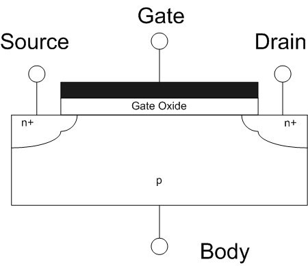
An equivalent oxide thickness usually given in nanometers (nm) is the thickness of silicon oxide film that provides the same electrical performance as that of a high-κ material being used. The term is often used when describing field effect transistors, which rely on an electrically insulating pad of material between a gate and a doped semiconducting region. Device performance has typically been improved by reducing the thickness of a silicon oxide insulating pad. As the thickness of the insulating pad approached 5–10 nm, leakage current became a problem and alternate materials were necessary. These new materials had a lower equivalent oxide thickness so they could retain an appropriate gate oxide thickness to prevent leakage current while also increasing the switching speed. For example, a high-κ material with dielectric constant of 39 (compared to 3.9 for silicon oxide) would be ten times thicker than that of silicon oxide, helping to reduce the leakage of electrons acro ... [...More Info...] [...Related Items...] OR: [Wikipedia] [Google] [Baidu] |
Nanometer
330px, Different lengths as in respect to the molecular scale. The nanometre (international spelling as used by the International Bureau of Weights and Measures; SI symbol: nm) or nanometer (American and British English spelling differences#-re, -er, American spelling) is a units of measurement, unit of length in the International System of Units (SI), equal to one billionth ( short scale) of a metre () and to 1000 picometres. One nanometre can be expressed in scientific notation as , and as metres. History The nanometre was formerly known as the millimicrometre – or, more commonly, the millimicron for short – since it is of a micron (micrometre), and was often denoted by the symbol mμ or (more rarely and confusingly, since it logically should refer to a ''millionth'' of a micron) as μμ. Etymology The name combines the SI prefix '' nano-'' (from the Ancient Greek , ', "dwarf") with the parent unit name ''metre'' (from Greek , ', "unit of measuremen ... [...More Info...] [...Related Items...] OR: [Wikipedia] [Google] [Baidu] |
Silicon Oxide
Silicon oxide may refer to either of the following: *Silicon dioxide Silicon dioxide, also known as silica, is an oxide of silicon with the chemical formula , most commonly found in nature as quartz and in various living organisms. In many parts of the world, silica is the major constituent of sand. Silica is one ... or quartz, SiO2, very well characterized * Silicon monoxide, SiO, not very well characterized {{Short pages monitor ... [...More Info...] [...Related Items...] OR: [Wikipedia] [Google] [Baidu] |
High-κ Dielectric
The term high-κ dielectric refers to a material with a high dielectric constant (κ, kappa), as compared to silicon dioxide. High-κ dielectrics are used in semiconductor manufacturing processes where they are usually used to replace a silicon dioxide gate dielectric or another dielectric layer of a device. The implementation of high-κ gate dielectrics is one of several strategies developed to allow further miniaturization of microelectronic components, colloquially referred to as extending Moore's Law. Sometimes these materials are called "high-k" (pronounced "high kay"), instead of "high-κ" (high kappa). Need for high-κ materials Silicon dioxide () has been used as a gate oxide material for decades. As metal-oxide-semiconductor field-effect transistors (MOSFETs) have decreased in size, the thickness of the silicon dioxide gate dielectric has steadily decreased to increase the gate capacitance (per unit area) and thereby drive current (per device width), raising device pe ... [...More Info...] [...Related Items...] OR: [Wikipedia] [Google] [Baidu] |
Field Effect Transistor
The field-effect transistor (FET) is a type of transistor that uses an electric field to control the flow of current in a semiconductor. FETs ( JFETs or MOSFETs) are devices with three terminals: ''source'', ''gate'', and ''drain''. FETs control the flow of current by the application of a voltage to the gate, which in turn alters the conductivity between the drain and source. FETs are also known as unipolar transistors since they involve single-carrier-type operation. That is, FETs use either electrons (n-channel) or holes (p-channel) as charge carriers in their operation, but not both. Many different types of field effect transistors exist. Field effect transistors generally display very high input impedance at low frequencies. The most widely used field-effect transistor is the MOSFET (metal-oxide-semiconductor field-effect transistor). History The concept of a field-effect transistor (FET) was first patented by Austro-Hungarian physicist Julius Edgar Lilienfeld in 1 ... [...More Info...] [...Related Items...] OR: [Wikipedia] [Google] [Baidu] |
Doping (semiconductor)
In semiconductor production, doping is the intentional introduction of impurities into an intrinsic semiconductor for the purpose of modulating its electrical, optical and structural properties. The doped material is referred to as an extrinsic semiconductor. Small numbers of dopant atoms can change the ability of a semiconductor to conduct electricity. When on the order of one dopant atom is added per 100 million atoms, the doping is said to be ''low'' or ''light''. When many more dopant atoms are added, on the order of one per ten thousand atoms, the doping is referred to as ''high'' or ''heavy''. This is often shown as ''n+'' for n-type doping or ''p+'' for p-type doping. (''See the article on semiconductors for a more detailed description of the doping mechanism.'') A semiconductor doped to such high levels that it acts more like a conductor than a semiconductor is referred to as a degenerate semiconductor. A semiconductor can be considered i-type semiconductor if it ha ... [...More Info...] [...Related Items...] OR: [Wikipedia] [Google] [Baidu] |
Semiconductor
A semiconductor is a material which has an electrical conductivity value falling between that of a conductor, such as copper, and an insulator, such as glass. Its resistivity falls as its temperature rises; metals behave in the opposite way. Its conducting properties may be altered in useful ways by introducing impurities ("doping") into the crystal structure. When two differently doped regions exist in the same crystal, a semiconductor junction is created. The behavior of charge carriers, which include electrons, ions, and electron holes, at these junctions is the basis of diodes, transistors, and most modern electronics. Some examples of semiconductors are silicon, germanium, gallium arsenide, and elements near the so-called "metalloid staircase" on the periodic table. After silicon, gallium arsenide is the second-most common semiconductor and is used in laser diodes, solar cells, microwave-frequency integrated circuits, and others. Silicon is a critical element for ... [...More Info...] [...Related Items...] OR: [Wikipedia] [Google] [Baidu] |
Dielectric Constant
The relative permittivity (in older texts, dielectric constant) is the permittivity of a material expressed as a ratio with the electric permittivity of a vacuum. A dielectric is an insulating material, and the dielectric constant of an insulator measures the ability of the insulator to store electric energy in an electrical field. Permittivity is a material's property that affects the Coulomb force between two point charges in the material. Relative permittivity is the factor by which the electric field between the charges is decreased relative to vacuum. Likewise, relative permittivity is the ratio of the capacitance of a capacitor using that material as a dielectric, compared with a similar capacitor that has vacuum as its dielectric. Relative permittivity is also commonly known as the dielectric constant, a term still used but deprecated by standards organizations in engineering as well as in chemistry. Definition Relative permittivity is typically denoted as (sometimes ... [...More Info...] [...Related Items...] OR: [Wikipedia] [Google] [Baidu] |
Capacitance
Capacitance is the capability of a material object or device to store electric charge. It is measured by the change in charge in response to a difference in electric potential, expressed as the ratio of those quantities. Commonly recognized are two closely related notions of capacitance: ''self capacitance'' and ''mutual capacitance''. An object that can be electrically charged exhibits self capacitance, for which the electric potential is measured between the object and ground. Mutual capacitance is measured between two components, and is particularly important in the operations of the capacitor, a device designed for this purpose as an elementary linear electronic component. Capacitance is a function only of the geometry of the design of the capacitor, e.g., the opposing surface area of the plates and the distance between them, and the permittivity of the dielectric material between the plates. For many dielectric materials, the permittivity and thus the capacitance, is ... [...More Info...] [...Related Items...] OR: [Wikipedia] [Google] [Baidu] |
Hafnium Oxide
Hafnium(IV) oxide is the inorganic compound with the formula . Also known as hafnium dioxide or hafnia, this colourless solid is one of the most common and stable compounds of hafnium. It is an electrical insulator with a band gap of 5.3~5.7 eV. Hafnium dioxide is an intermediate in some processes that give hafnium metal. Hafnium(IV) oxide is quite inert. It reacts with strong acids such as concentrated sulfuric acid and with strong bases. It dissolves slowly in hydrofluoric acid to give fluorohafnate anions. At elevated temperatures, it reacts with chlorine in the presence of graphite or carbon tetrachloride to give hafnium tetrachloride. Structure Hafnia typically adopts the same structure as zirconia (ZrO2). Unlike TiO2, which features six-coordinate Ti in all phases, zirconia and hafnia consist of seven-coordinate metal centres. A variety of other crystalline phases have been experimentally observed, including cubic fluorite (Fmm), tetragonal (P42/nmc), monoclinic (P21/c ... [...More Info...] [...Related Items...] OR: [Wikipedia] [Google] [Baidu] |
Multigate Device
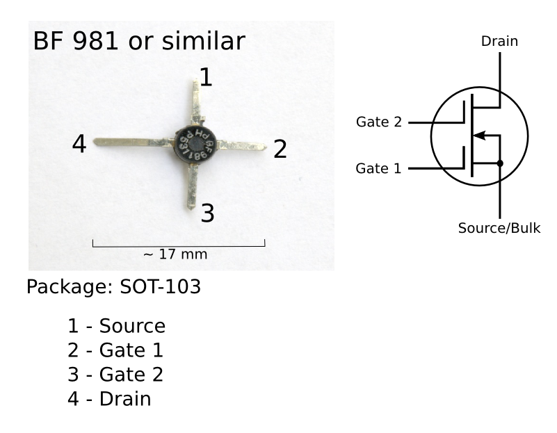
A multigate device, multi-gate MOSFET or multi-gate field-effect transistor (MuGFET) refers to a metal–oxide–semiconductor field-effect transistor (MOSFET) that has more than one gate on a single transistor. The multiple gates may be controlled by a single gate electrode, wherein the multiple gate surfaces act electrically as a single gate, or by independent gate electrodes. A multigate device employing independent gate electrodes is sometimes called a multiple-independent-gate field-effect transistor (MIGFET). The most widely used multi-gate devices are the FinFET (fin field-effect transistor) and the GAAFET (gate-all-around field-effect transistor), which are non-planar transistors, or 3D transistors. Multi-gate transistors are one of the several strategies being developed by MOS semiconductor manufacturers to create ever-smaller microprocessors and memory cells, colloquially referred to as extending Moore's law (in its narrow, specific version concerning density scaling ... [...More Info...] [...Related Items...] OR: [Wikipedia] [Google] [Baidu] |


