Integrated Circuit Layout on:
[Wikipedia]
[Google]
[Amazon]
 In
In
"Managing More-than-Moore Integration Technology Development"
2018. p. 99
 In
In integrated circuit design
Integrated circuit design, semiconductor design, chip design or IC design, is a sub-field of electronics engineering, encompassing the particular Boolean logic, logic and circuit design techniques required to design integrated circuits (ICs). A ...
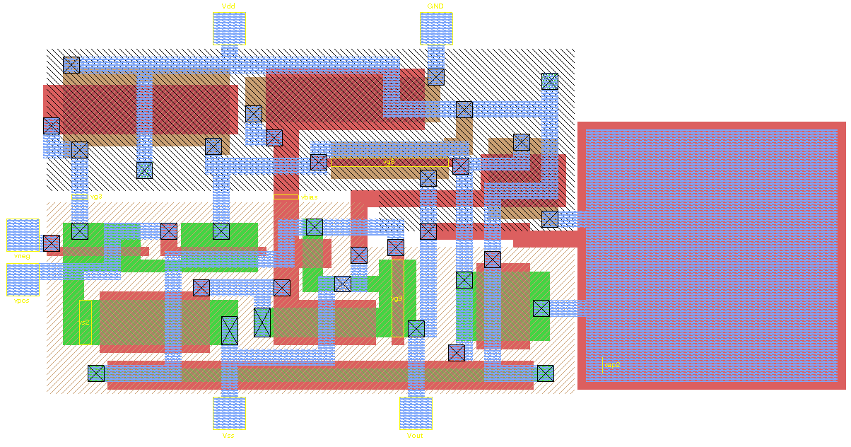
, integrated circuit (IC) layout, also known IC mask layout or mask design, is the representation of an integrated circuit
An integrated circuit (IC), also known as a microchip or simply chip, is a set of electronic circuits, consisting of various electronic components (such as transistors, resistors, and capacitors) and their interconnections. These components a ...
in terms of planar geometric shape
A shape is a graphical representation of an object's form or its external boundary, outline, or external surface. It is distinct from other object properties, such as color, texture, or material type.
In geometry, ''shape'' excludes informat ...
s which correspond to the patterns of metal
A metal () is a material that, when polished or fractured, shows a lustrous appearance, and conducts electrical resistivity and conductivity, electricity and thermal conductivity, heat relatively well. These properties are all associated wit ...
, oxide
An oxide () is a chemical compound containing at least one oxygen atom and one other element in its chemical formula. "Oxide" itself is the dianion (anion bearing a net charge of −2) of oxygen, an O2− ion with oxygen in the oxidation st ...
, or semiconductor
A semiconductor is a material with electrical conductivity between that of a conductor and an insulator. Its conductivity can be modified by adding impurities (" doping") to its crystal structure. When two regions with different doping level ...
layers that make up the components of the integrated circuit. Originally the overall process was called tapeout, as historically early ICs used graphical black crepe tape on mylar
BoPET (biaxially oriented polyethylene terephthalate) is a polyester film made from stretched polyethylene terephthalate (PET) and is used for its high tensile strength, chemical stability, dimensional stability, transparency reflectivity, an ...
media for photo imaging (erroneously believed to reference magnetic data—the photo process greatly predated magnetic media).
When using a standard process—where the interaction of the many chemical, thermal, and photographic variables is known and carefully controlled—the behaviour of the final integrated circuit depends largely on the positions and interconnections of the geometric shapes. Using a computer-aided layout tool, the layout engineer—or layout technician—places and connects all of the components that make up the chip such that they meet certain criteria—typically: performance, size, density, and manufacturability. This practice is often subdivided between two primary layout disciplines: analog and digital
Digital usually refers to something using discrete digits, often binary digits.
Businesses
*Digital bank, a form of financial institution
*Digital Equipment Corporation (DEC) or Digital, a computer company
*Digital Research (DR or DRI), a software ...
.
The generated layout must pass a series of checks in a process known as physical verification. The most common checks in this verification process are
* Design rule checking (DRC),
* Layout versus schematic (LVS),
* parasitic extraction,
* antenna rule checking, and
* electrical rule checking (ERC).
When all verification is complete, layout post processing is applied where the data is also translated into an industry-standard format, typically GDSII, and sent to a semiconductor foundry. The milestone completion of the layout process of sending this data to the foundry is now colloquially called "tapeout". The foundry converts the data into mask data and uses it to generate the photomask
A photomask (also simply called a mask) is an opaque plate with transparent areas that allow light to shine through in a defined pattern. Photomasks are commonly used in photolithography for the production of integrated circuits (ICs or "chips") ...
s used in a photolithographic process of semiconductor device fabrication
Semiconductor device fabrication is the process used to manufacture semiconductor devices, typically integrated circuits (ICs) such as microprocessors, microcontrollers, and memories (such as Random-access memory, RAM and flash memory). It is a ...
.
In the earlier, simpler, days of IC design, layout was done by hand using opaque tapes and films, an evolution derived from early days of printed circuit board
A printed circuit board (PCB), also called printed wiring board (PWB), is a Lamination, laminated sandwich structure of electrical conduction, conductive and Insulator (electricity), insulating layers, each with a pattern of traces, planes ...
(PCB) design -- tape-out.
Modern IC layout is done with the aid of IC layout editor software, mostly automatically using EDA tools, including place and route
Place and route (also called PnR or P&R) is a stage in the design of printed circuit boards, integrated circuits, and field-programmable gate arrays. As implied by the name, it is composed of two steps, placement and routing. The first step, p ...
tools or schematic-driven layout tools.
Typically this involves a library of standard cells.
The manual operation of choosing and positioning the geometric shapes is informally known as "polygon
In geometry, a polygon () is a plane figure made up of line segments connected to form a closed polygonal chain.
The segments of a closed polygonal chain are called its '' edges'' or ''sides''. The points where two edges meet are the polygon ...
pushing".
Riko Radojcic"Managing More-than-Moore Integration Technology Development"
2018. p. 99
See also
* Interconnects (integrated circuits) * Physical design (electronics) *Printed circuit board
A printed circuit board (PCB), also called printed wiring board (PWB), is a Lamination, laminated sandwich structure of electrical conduction, conductive and Insulator (electricity), insulating layers, each with a pattern of traces, planes ...
* Integrated circuit design
Integrated circuit design, semiconductor design, chip design or IC design, is a sub-field of electronics engineering, encompassing the particular Boolean logic, logic and circuit design techniques required to design integrated circuits (ICs). A ...
* Floorplan (microelectronics)
In electronic design automation, a floorplan of an integrated circuit consists of a schematic arrangement of its major functional blocks on the chip area and the specification of high-level parameters such as the aspect ratio or core utilization. ...
References
Further reading
*Clein, D. (2000). ''CMOS IC Layout''. Newnes. *Hastings, A. (2005). ''The Art of Analog Layout''. Prentice Hall. * *Saint, Ch. and J. (2002). ''IC Layout Basics''. McGraw-Hill. {{ISBN, 0-07-138625-4 Electronic design Electronic design automation Integrated circuits