|
Hydrogen-terminated Silicon Surface
Hydrogen-terminated silicon surface is a chemically passivated silicon substrate where the surface Si atoms are bonded to hydrogen. The hydrogen-terminated surfaces are hydrophobic, luminescent, and amenable to chemical modification. Hydrogen-terminated silicon is an intermediate in the growth of bulk silicon from silane: :SiH4 → Si + 2H2 Preparation Silicon wafers are treated with solutions of electronic-grade hydrofluoric acid in water, buffered water, or alcohol. One of the relevant reactions is simply removal of silicon oxides: :SiO2 + 4 HF → SiF4 + 2 H2O The key reaction however is the formation of the hydrosilane functional group. atomic force microscope (AFM) has been used to manipulate hydrogen-terminated silicon surfaces. Properties Hydrogen termination removes dangling bonds. All surface Si atoms are tetrahedral. Hydrogen termination confers stability in ambient environments. So again, the surface is both clean (of oxides) and relatively inert. Th ... [...More Info...] [...Related Items...] OR: [Wikipedia] [Google] [Baidu] |
Silicon
Silicon is a chemical element with the symbol Si and atomic number 14. It is a hard, brittle crystalline solid with a blue-grey metallic luster, and is a tetravalent metalloid and semiconductor. It is a member of group 14 in the periodic table: carbon is above it; and germanium, tin, lead, and flerovium are below it. It is relatively unreactive. Because of its high chemical affinity for oxygen, it was not until 1823 that Jöns Jakob Berzelius was first able to prepare it and characterize it in pure form. Its oxides form a family of anions known as silicates. Its melting and boiling points of 1414 °C and 3265 °C, respectively, are the second highest among all the metalloids and nonmetals, being surpassed only by boron. Silicon is the eighth most common element in the universe by mass, but very rarely occurs as the pure element in the Earth's crust. It is widely distributed in space in cosmic dusts, planetoids, and planets as various forms of silicon ... [...More Info...] [...Related Items...] OR: [Wikipedia] [Google] [Baidu] |
Diazo
The diazo group is an organic moiety consisting of two linked nitrogen atoms ( azo) at the terminal position. Overall charge neutral organic compounds containing the diazo group bound to a carbon atom are called diazo compounds or diazoalkanes and are described by the general structural formula R2C=N+=N–. The simplest example of a diazo compound is diazomethane, CH2N2. Diazo compounds (R2C=N2) should not be confused with azo compounds of the type R-N=N-R or with diazonium compounds of the type R-N2+. Structure The electronic structure of diazo compounds is characterized by π electron density delocalized over the α-carbon and two nitrogen atoms, along with an orthogonal π system with electron density delocalized over only the terminal nitrogen atoms. Because all octet rule-satisfying resonance forms of diazo compounds have formal charges, they are members of a class of compounds known as 1,3-dipoles. Some of the most stable diazo compounds are α-diazo-β-diketones ... [...More Info...] [...Related Items...] OR: [Wikipedia] [Google] [Baidu] |
Thin Films
A thin film is a layer of material ranging from fractions of a nanometer ( monolayer) to several micrometers in thickness. The controlled synthesis of materials as thin films (a process referred to as deposition) is a fundamental step in many applications. A familiar example is the household mirror, which typically has a thin metal coating on the back of a sheet of glass to form a reflective interface. The process of silvering was once commonly used to produce mirrors, while more recently the metal layer is deposited using techniques such as sputtering. Advances in thin film deposition techniques during the 20th century have enabled a wide range of technological breakthroughs in areas such as magnetic recording media, electronic semiconductor devices, integrated passive devices, LEDs, optical coatings (such as antireflective coatings), hard coatings on cutting tools, and for both energy generation (e.g. thin-film solar cells) and storage ( thin-film batteries). It is al ... [...More Info...] [...Related Items...] OR: [Wikipedia] [Google] [Baidu] |
Nanotechnology
Nanotechnology, also shortened to nanotech, is the use of matter on an atomic, molecular, and supramolecular scale for industrial purposes. The earliest, widespread description of nanotechnology referred to the particular technological goal of precisely manipulating atoms and molecules for fabrication of macroscale products, also now referred to as molecular nanotechnology. A more generalized description of nanotechnology was subsequently established by the National Nanotechnology Initiative, which defined nanotechnology as the manipulation of matter with at least one dimension sized from 1 to 100 nanometers (nm). This definition reflects the fact that quantum mechanical effects are important at this quantum-realm scale, and so the definition shifted from a particular technological goal to a research category inclusive of all types of research and technologies that deal with the special properties of matter which occur below the given size threshold. It is therefore commo ... [...More Info...] [...Related Items...] OR: [Wikipedia] [Google] [Baidu] |
Materials
Material is a substance or mixture of substances that constitutes an object. Materials can be pure or impure, living or non-living matter. Materials can be classified on the basis of their physical and chemical properties, or on their geological origin or biological function. Materials science is the study of materials, their properties and their applications. Raw materials can be processed in different ways to influence their properties, by purification, shaping or the introduction of other materials. New materials can be produced from raw materials by synthesis. In industry, materials are inputs to manufacturing processes to produce products or more complex materials. Historical elements Materials chart the history of humanity. The system of the three prehistoric ages (Stone Age, Bronze Age, Iron Age) were succeeded by historical ages: steel age in the 19th century, polymer age in the middle of the following century (plastic age) and silicon age in the second half of the 20 ... [...More Info...] [...Related Items...] OR: [Wikipedia] [Google] [Baidu] |
Silanization Of Silicon And Mica
Silanization of silicon and mica is the coating of these materials with a thin layer of self assembling units. Biological applications of silanization Nanoscale analysis of proteins using atomic force microscopy (AFM) requires surfaces with well-defined topologies and chemistries for many experimental techniques. Biomolecules, particularly proteins, can be immobilized simply on an unmodified substrate surface through hydrophobic or electrostatic interactions. However, several problems are associated with physical adsorption of proteins on surfaces. With metal surfaces, protein denaturation, unstable and reversible binding, nonspecific and random immobilization of protein have been reported. One alternative involves the interaction of chemically modified surfaces with proteins under non-denaturing circumstances. Chemical modification of surfaces provides the potential to precisely control the chemistry of the surface, and with the correct chemical modifications, there are several ... [...More Info...] [...Related Items...] OR: [Wikipedia] [Google] [Baidu] |
Quantum Dot
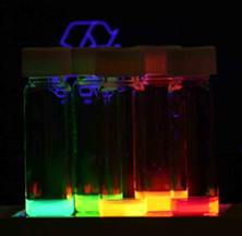
Quantum dots (QDs) are semiconductor particles a few nanometres in size, having optical and electronic properties that differ from those of larger particles as a result of quantum mechanics. They are a central topic in nanotechnology. When the quantum dots are illuminated by UV light, an electron in the quantum dot can be excited to a state of higher energy. In the case of a semiconducting quantum dot, this process corresponds to the transition of an electron from the valence band to the conductance band. The excited electron can drop back into the valence band releasing its energy as light. This light emission (photoluminescence) is illustrated in the figure on the right. The color of that light depends on the energy difference between the conductance band and the valence band, or the transition between discrete energy states when band structure is no longer a good definition in QDs. In the language of materials science, nanoscale semiconductor materials tightly confine either ... [...More Info...] [...Related Items...] OR: [Wikipedia] [Google] [Baidu] |
Infrared Spectrum
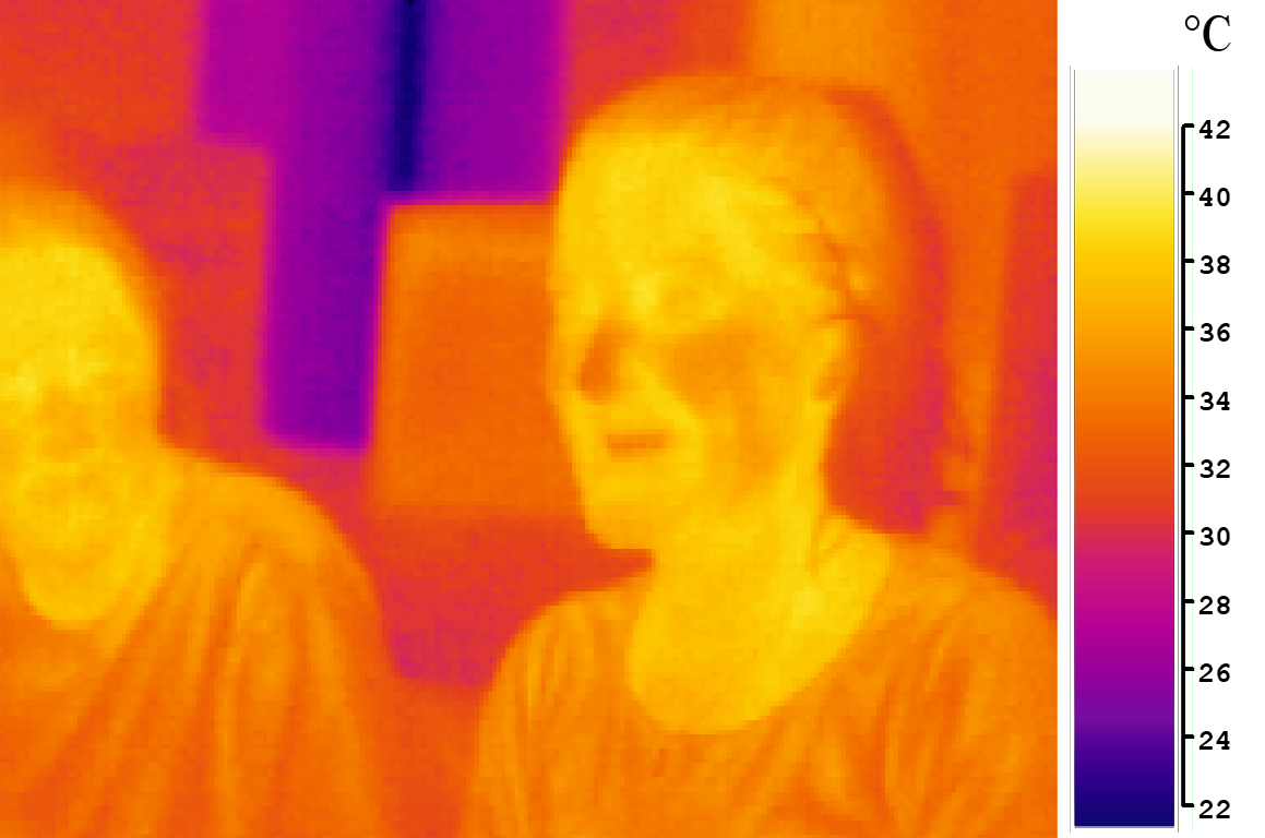
Infrared (IR), sometimes called infrared light, is electromagnetic radiation (EMR) with wavelengths longer than those of visible light. It is therefore invisible to the human eye. IR is generally understood to encompass wavelengths from around 1 millimeter (300 GHz) to the nominal red edge of the visible spectrum, around 700 nanometers (430 THz). Longer IR wavelengths (30 μm-100 μm) are sometimes included as part of the terahertz radiation range. Almost all black-body radiation from objects near room temperature is at infrared wavelengths. As a form of electromagnetic radiation, IR propagates energy and momentum, exerts radiation pressure, and has properties corresponding to both those of a wave and of a particle, the photon. It was long known that fires emit invisible heat; in 1681 the pioneering experimenter Edme Mariotte showed that glass, though transparent to sunlight, obstructed radiant heat. In 1800 the astronomer Sir William Herschel discovered tha ... [...More Info...] [...Related Items...] OR: [Wikipedia] [Google] [Baidu] |
Hydrosilylation
Hydrosilylation, also called catalytic hydrosilation, describes the addition of Si-H bonds across unsaturated bonds."Hydrosilylation A Comprehensive Review on Recent Advances" B. Marciniec (ed.), Advances in Silicon Science, Springer Science, 2009. Ordinarily the reaction is conducted catalytically and usually the substrates are unsaturated organic compounds. Alkenes and alkynes give alkyl and vinyl silanes; aldehydes and ketones give silyl ethers. Hydrosilylation has been called the "most important application of platinum in homogeneous catalysis." Scope and mechanism Hydrosilylation of alkenes represents a commercially important method for preparing organosilicon compounds. The process is mechanistically similar to the hydrogenation of alkenes. In fact, similar catalysts are sometimes employed for the two catalytic processes. The prevalent mechanism, called the Chalk-Harrod mechanism, assumes an intermediate metal complex that contains a hydride, a silyl ligand (R3Si), and ... [...More Info...] [...Related Items...] OR: [Wikipedia] [Google] [Baidu] |
Alkene
In organic chemistry, an alkene is a hydrocarbon containing a carbon–carbon double bond. Alkene is often used as synonym of olefin, that is, any hydrocarbon containing one or more double bonds.H. Stephen Stoker (2015): General, Organic, and Biological Chemistry'. 1232 pages. Two general types of monoalkenes are distinguished: terminal and internal. Also called α-olefins, terminal alkenes are more useful. However, the International Union of Pure and Applied Chemistry (IUPAC) recommends using the name "alkene" only for acyclic hydrocarbons with just one double bond; alkadiene, alkatriene, etc., or polyene for acyclic hydrocarbons with two or more double bonds; cycloalkene, cycloalkadiene, etc. for cyclic ones; and "olefin" for the general class – cyclic or acyclic, with one or more double bonds. Acyclic alkenes, with only one double bond and no other functional groups (also known as mono-enes) form a homologous series of hydrocarbons with the general formula wit ... [...More Info...] [...Related Items...] OR: [Wikipedia] [Google] [Baidu] |
Wafer (electronics)
In electronics, a wafer (also called a slice or substrate) is a thin slice of semiconductor, such as a crystalline silicon (c-Si), used for the fabrication of integrated circuits and, in photovoltaics, to manufacture solar cells. The wafer serves as the substrate for microelectronic devices built in and upon the wafer. It undergoes many microfabrication processes, such as doping, ion implantation, etching, thin-film deposition of various materials, and photolithographic patterning. Finally, the individual microcircuits are separated by wafer dicing and packaged as an integrated circuit. History In the semiconductor or silicon wafer industry, the term wafer appeared in the 1950s to describe a thin round slice of semiconductor material, typically germanium or silicon. Round shape comes from single-crystal ingots usually produced using the Czochralski method. Silicon wafers were first introduced in the 1940s. By 1960, silicon wafers were being manufactured in the U.S. by c ... [...More Info...] [...Related Items...] OR: [Wikipedia] [Google] [Baidu] |
Chemically Inert
In chemistry, the term chemically inert is used to describe a substance that is not chemically reactive. From a thermodynamic perspective, a substance is inert, or nonlabile, if it is thermodynamically unstable (positive standard Gibbs free energy of formation) yet decomposes at a slow, or negligible rate. Most of the noble gases, which appear in the last column of the periodic table, are classified as inert (or unreactive). These elements are stable in their naturally occurring form (gaseous form) and they are called inert gases. Noble gas The noble gases ( helium, neon, argon, krypton, xenon and radon) were previously known as 'inert gases' because of their perceived lack of participation in any chemical reactions. The reason for this is that their outermost electron shells (valence shells) are completely filled, so that they have little tendency to gain or lose electrons. They are said to acquire a noble gas configuration, or a full electron configuration. It is no ... [...More Info...] [...Related Items...] OR: [Wikipedia] [Google] [Baidu] |

_250_nm_by_250_nm_image_of_one-atom-thick_silver_islands_grown_on_palladium_(111)_surface.png)


