|
Graphene Nanoribbons
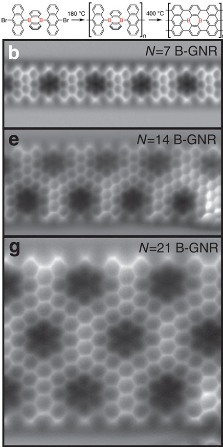
Graphene nanoribbons (GNRs, also called nano-graphene ribbons or nano-graphite ribbons) are strips of graphene with width less than 100 nm. Graphene ribbons were introduced as a theoretical model by Mitsutaka Fujita and coauthors to examine the edge and nanoscale size effect in graphene. Some earlier studies of graphitic ribbons within the area of conductive polymers in the field of synthetic metals include works by Kazuyoshi Tanaka, Tokio Yamabe and co-authors, Steven Kivelson and Douglas J. Klein. While Tanaka, Yamabe and Kivelson studied so-called zigzag and armchair edges of graphite, Klein introduced a different edge geometry that is frequently referred to as a bearded edge. Production Nanotomy Large quantities of width-controlled GNRs can be produced via graphite nanotomy, where applying a sharp diamond knife on graphite produces graphite nanoblocks, which can then be exfoliated to produce GNRs as shown by Vikas Berry. GNRs can also be produced by "unzipping" or ... [...More Info...] [...Related Items...] OR: [Wikipedia] [Google] [Baidu] |
Band Gap
In solid-state physics and solid-state chemistry, a band gap, also called a bandgap or energy gap, is an energy range in a solid where no electronic states exist. In graphs of the electronic band structure of solids, the band gap refers to the energy difference (often expressed in electronvolts) between the top of the valence band and the bottom of the conduction band in insulators and semiconductors. It is the energy required to promote an electron from the valence band to the conduction band. The resulting conduction-band electron (and the electron hole in the valence band) are free to move within the crystal lattice and serve as charge carriers to conduct electric current. It is closely related to the HOMO/LUMO gap in chemistry. If the valence band is completely full and the conduction band is completely empty, then electrons cannot move within the solid because there are no available states. If the electrons are not free to move within the crystal lattice, then there ... [...More Info...] [...Related Items...] OR: [Wikipedia] [Google] [Baidu] |
Adatom
An adatom is an atom that lies on a crystal surface, and can be thought of as the opposite of a surface vacancy. This term is used in surface chemistry and epitaxy, when describing single atoms lying on surfaces and surface roughness. The word is a portmanteau of " adsorbed atom". A single atom, a cluster of atoms, or a molecule or cluster of molecules may all be referred to by the general term " adparticle". This is often a thermodynamically unfavorable state. However, cases such as graphene may provide counter-examples. Growth ″Adatom″ is a portmanteau word, short for adsorbed atom. When the atom arrives at a crystal surface, it is adsorbed by the periodic potential of the crystal, thus becoming an adatom. The minima of this potential form a network of adsorption sites on the surface. There are different types of adsorption sites. Each of these sites corresponds to a different structure of the surface. There are five different types of adsorption sites, which are: o ... [...More Info...] [...Related Items...] OR: [Wikipedia] [Google] [Baidu] |
Magnetic Moment
In electromagnetism, the magnetic moment or magnetic dipole moment is the combination of strength and orientation of a magnet or other object or system that exerts a magnetic field. The magnetic dipole moment of an object determines the magnitude of torque the object experiences in a given magnetic field. When the same magnetic field is applied, objects with larger magnetic moments experience larger torques. The strength (and direction) of this torque depends not only on the magnitude of the magnetic moment but also on its orientation relative to the direction of the magnetic field. Its direction points from the south pole to the north pole of the magnet (i.e., inside the magnet). The magnetic moment also expresses the magnetic force effect of a magnet. The magnetic field of a magnetic dipole is proportional to its magnetic dipole moment. The dipole component of an object's magnetic field is symmetric about the direction of its magnetic dipole moment, and decreases as the inverse ... [...More Info...] [...Related Items...] OR: [Wikipedia] [Google] [Baidu] |
Spin Polarization
In particle physics, spin polarization is the degree to which the spin, i.e., the intrinsic angular momentum of elementary particles, is aligned with a given direction. This property may pertain to the spin, hence to the magnetic moment, of conduction electrons in ferromagnetic metals, such as iron, giving rise to spin-polarized currents. It may refer to (static) spin waves, preferential correlation of spin orientation with ordered lattices (semiconductors or insulators). It may also pertain to beams of particles, produced for particular aims, such as polarized neutron scattering or muon spin spectroscopy. Spin polarization of electrons or of nuclei, often called simply magnetization, is also produced by the application of a magnetic field. Curie law is used to produce an induction signal in electron spin resonance (ESR or EPR) and in nuclear magnetic resonance (NMR). Spin polarization is also important for spintronics, a branch of electronics. Magnetic semiconducto ... [...More Info...] [...Related Items...] OR: [Wikipedia] [Google] [Baidu] |
Density Functional Theory
Density functional theory (DFT) is a computational quantum mechanical modelling method used in physics, chemistry and materials science to investigate the electronic structure (or nuclear structure) (principally the ground state) of many-body systems, in particular atoms, molecules, and the condensed phases. Using this theory, the properties of a many-electron system can be determined by using functionals - that is, functions that accept a function as input and output a single real number. In the case of DFT, these are functionals of the spatially dependent electron density. DFT is among the most popular and versatile methods available in condensed-matter physics, computational physics, and computational chemistry. DFT has been very popular for calculations in solid-state physics since the 1970s. However, DFT was not considered accurate enough for calculations in quantum chemistry until the 1990s, when the approximations used in the theory were greatly refined to better m ... [...More Info...] [...Related Items...] OR: [Wikipedia] [Google] [Baidu] |
Quantization (physics)
Quantization (in British English quantisation) is the systematic transition procedure from a classical understanding of physical phenomena to a newer understanding known as quantum mechanics. It is a procedure for constructing quantum mechanics from classical mechanics. A generalization involving infinite degrees of freedom is field quantization, as in the "quantization of the electromagnetic field", referring to photons as field " quanta" (for instance as light quanta). This procedure is basic to theories of atomic physics, chemistry, particle physics, nuclear physics, condensed matter physics, and quantum optics. Historical overview In 1901, when Max Planck was developing the distribution function of statistical mechanics to solve the ultraviolet catastrophe problem, he realized that the properties of blackbody radiation can be explained by the assumption that the amount of energy must be in countable fundamental units, i.e. amount of energy is not continuous but ... [...More Info...] [...Related Items...] OR: [Wikipedia] [Google] [Baidu] |
Scanning Tunneling Microscope
A scanning tunneling microscope (STM) is a type of scanning probe microscope used for imaging surfaces at the atomic level. Its development in 1981 earned its inventors, Gerd Binnig and Heinrich Rohrer, then at IBM Zürich, the Nobel Prize in Physics in 1986. STM senses the surface by using an extremely sharp conducting tip that can distinguish features smaller than 0.1 nm with a 0.01 nm (10 pm) depth resolution. This means that individual atoms can routinely be imaged and manipulated. Most scanning tunneling microscopes are built for use in ultra-high vacuum at temperatures approaching absolute zero, but variants exist for studies in air, water and other environments, and for temperatures over 1000 °C. STM is based on the concept of quantum tunneling. When the tip is brought very near to the surface to be examined, a bias voltage applied between the two allows electrons to tunnel through the vacuum separating them. The resulting ''tunneling current'' ... [...More Info...] [...Related Items...] OR: [Wikipedia] [Google] [Baidu] |
Vacuum
A vacuum (: vacuums or vacua) is space devoid of matter. The word is derived from the Latin adjective (neuter ) meaning "vacant" or "void". An approximation to such vacuum is a region with a gaseous pressure much less than atmospheric pressure. Physicists often discuss ideal test results that would occur in a ''perfect'' vacuum, which they sometimes simply call "vacuum" or free space, and use the term partial vacuum to refer to an actual imperfect vacuum as one might have in a laboratory or in space. In engineering and applied physics on the other hand, vacuum refers to any space in which the pressure is considerably lower than atmospheric pressure. The Latin term ''in vacuo'' is used to describe an object that is surrounded by a vacuum. The ''quality'' of a partial vacuum refers to how closely it approaches a perfect vacuum. Other things equal, lower gas pressure means higher-quality vacuum. For example, a typical vacuum cleaner produces enough suction to reduce air pressur ... [...More Info...] [...Related Items...] OR: [Wikipedia] [Google] [Baidu] |
Electron Mobility
In solid-state physics, the electron mobility characterizes how quickly an electron can move through a metal or semiconductor when pushed or pulled by an electric field. There is an analogous quantity for Electron hole, holes, called hole mobility. The term carrier mobility refers in general to both electron and hole mobility. Electron and hole mobility are special cases of electrical mobility of charged particles in a fluid under an applied electric field. When an electric field ''E'' is applied across a piece of material, the electrons respond by moving with an average velocity called the drift velocity, v_d. Then the electron mobility ''μ'' is defined as v_d = \mu E. Electron mobility is almost always specified in units of square centimetre, cm2/(volt, V⋅second, s). This is different from the SI unit of mobility, square metre, m2/(volt, V⋅second, s). They are related by 1 m2/(V⋅s) = 104 cm2/(V⋅s). Electrical resistivity and conductivity, Conductivity is proportiona ... [...More Info...] [...Related Items...] OR: [Wikipedia] [Google] [Baidu] |
Field Effect Transistor
The field-effect transistor (FET) is a type of transistor that uses an electric field to control the current through a semiconductor. It comes in two types: junction FET (JFET) and metal-oxide-semiconductor FET (MOSFET). FETs have three terminals: ''source'', ''gate'', and ''drain''. FETs control the current by the application of a voltage to the gate, which in turn alters the conductivity between the drain and source. FETs are also known as unipolar transistors since they involve single-carrier-type operation. That is, FETs use either electrons (n-channel) or holes (p-channel) as charge carriers in their operation, but not both. Many different types of field effect transistors exist. Field effect transistors generally display very high input impedance at low frequencies. The most widely used field-effect transistor is the MOSFET (metal–oxide–semiconductor field-effect transistor). History The concept of a field-effect transistor (FET) was first patented by the Aust ... [...More Info...] [...Related Items...] OR: [Wikipedia] [Google] [Baidu] |
Chemical Vapour Deposition
Chemical vapor deposition (CVD) is a vacuum deposition method used to produce high-quality, and high-performance, solid materials. The process is often used in the semiconductor industry to produce thin films. In typical CVD, the wafer (substrate) is exposed to one or more volatile precursors, which react and/or decompose on the substrate surface to produce the desired deposit. Frequently, volatile by-products are also produced, which are removed by gas flow through the reaction chamber. Microfabrication processes widely use CVD to deposit materials in various forms, including: monocrystalline, polycrystalline, amorphous, and epitaxial. These materials include: silicon ( dioxide, carbide, nitride, oxynitride), carbon (fiber, nanofibers, nanotubes, diamond and graphene), fluorocarbons, filaments, tungsten, titanium nitride and various high-κ dielectrics. The term ''chemical vapour deposition'' was coined in 1960 by ''John M. Blocher, Jr.'' who intended to different ... [...More Info...] [...Related Items...] OR: [Wikipedia] [Google] [Baidu] |


