|
Coordinatograph
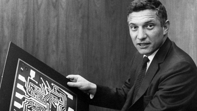
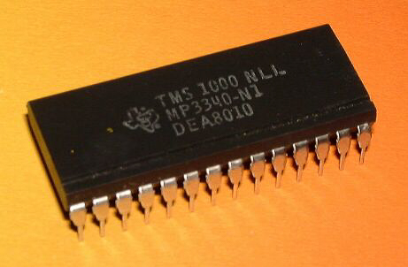
A coordinatograph is an instrument that mechanically plots X and Y coordinates onto a surface, such as in compiling maps or in plotting control points such as in electronic circuit design. One historic application of a coordinatograph was a machine that precisely placed and cut rubylith to create photomasks for early integrated circuits, including some of the earliest generations of the modern microprocessors used in personal computers. The coordinatograph produced layout would then be photographically reduced 100:1 to create the production photomask. See also * Cartography * Photolithography * Etching (microfabrication) * Design for manufacturability * Semiconductor device fabrication References External links * https://www.cnet.com/news/intels-accidental-revolution states rubylith was used on the Intel 4004 The Intel 4004 was part of the 4 chip MCS-4 micro computer set, released by the Intel, Intel Corporation in November 1971; the 4004 being part of the first commercia ... [...More Info...] [...Related Items...] OR: [Wikipedia] [Google] [Baidu] |
Rubylith
Rubylith is a brand of Photomask, masking film, invented and trademarked by the Ulano Corporation. Today the brand has become Genericized trademark, genericized to the point that it has become synonymous with all coloured masking films. Rubylith consists of two films sandwiched together. The bottom layer is a clear polyester backing sheet; the top layer is a Transparency (optics), translucent, red-(ruby-)coloured sheet. The top layer can be cut and peeled away from the bottom layer. The top layer's colour is light-safe for Orthochromasia#Orthochromatic_photography, orthochromatic films (which are sensitive to blue and green light but insensitive to red light). Rubylith is used in many areas of graphic design, typically to produce masks for various printing techniques. For example it is often used to mask off areas of a design when using a photoresist to produce printing plates for offset lithography or gravure. It is also frequently used during screen-printing. Ulano also produ ... [...More Info...] [...Related Items...] OR: [Wikipedia] [Google] [Baidu] |
Cartography
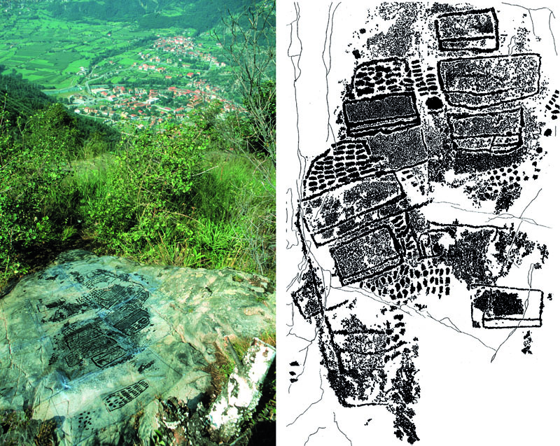
Cartography (; from , 'papyrus, sheet of paper, map'; and , 'write') is the study and practice of making and using maps. Combining science, aesthetics and technique, cartography builds on the premise that reality (or an imagined reality) can be modeled in ways that communicate spatial information effectively. The fundamental objectives of traditional cartography are to: * Set the map's agenda and select traits of the object to be mapped. This is the concern of map editing. Traits may be physical, such as roads or land masses, or may be abstract, such as toponyms or political boundaries. * Represent the terrain of the mapped object on flat media. This is the concern of map projections. * Eliminate the mapped object's characteristics that are irrelevant to the map's purpose. This is the concern of Cartographic generalization, generalization. * Reduce the complexity of the characteristics that will be mapped. This is also the concern of generalization. * Orchestrate the elements ... [...More Info...] [...Related Items...] OR: [Wikipedia] [Google] [Baidu] |
Photomask
A photomask (also simply called a mask) is an opaque plate with transparent areas that allow light to shine through in a defined pattern. Photomasks are commonly used in photolithography for the production of integrated circuits (ICs or "chips") to produce a pattern on a thin wafer of material (usually silicon). In semiconductor manufacturing, a mask is sometimes called a reticle. In photolithography, several masks are used in turn, each one reproducing a layer of the completed design, and together known as a mask set. A curvilinear photomask has patterns with curves, which is a departure from conventional photomasks which only have patterns that are completely vertical or horizontal, known as manhattan geometry. These photomasks require special equipment to manufacture. History For IC production in the 1960s and early 1970s, an opaque rubylith film laminated onto a transparent mylar sheet was used. The design of one layer was cut into the rubylith, initially by hand on an i ... [...More Info...] [...Related Items...] OR: [Wikipedia] [Google] [Baidu] |
Integrated Circuit
An integrated circuit (IC), also known as a microchip or simply chip, is a set of electronic circuits, consisting of various electronic components (such as transistors, resistors, and capacitors) and their interconnections. These components are etched onto a small, flat piece ("chip") of semiconductor material, usually silicon. Integrated circuits are used in a wide range of electronic devices, including computers, smartphones, and televisions, to perform various functions such as processing and storing information. They have greatly impacted the field of electronics by enabling device miniaturization and enhanced functionality. Integrated circuits are orders of magnitude smaller, faster, and less expensive than those constructed of discrete components, allowing a large transistor count. The IC's mass production capability, reliability, and building-block approach to integrated circuit design have ensured the rapid adoption of standardized ICs in place of designs using discre ... [...More Info...] [...Related Items...] OR: [Wikipedia] [Google] [Baidu] |
List Of Intel Microprocessors
This generational list of Intel processors attempts to present all of Intel's processors from the 4-bit 4004 (1971) to the present high-end offerings. Concise technical data is given for each product. Latest 15th generation Core Desktop - Core Ultra Series 2 (codenamed " Arrow Lake") Released on October 24, 2024. It follows on from Meteor Lake which saw Intel move from monolithic silicon to a disaggregated MCM design. Meteor Lake was limited to a mobile release while Arrow Lake includes desktop processors and mobile processors. Desktop - Arrow Lake-S Mobile - Arrow Lake-U Arrow Lake-U uses refreshed Meteor Lake silicon fabricated on the Intel 3 node. Mobile - Arrow Lake-H Mobile - Arrow Lake-HX 13th and 14th generation Core Desktop - Raptor Lake-S Refresh (codenamed "Raptor Lake") (14th Gen) An iterative refresh of Raptor Lake-S desktop processors, called the 14th generation of Intel Core, was launched on October 17, 2023. CPUs in bold below ... [...More Info...] [...Related Items...] OR: [Wikipedia] [Google] [Baidu] |
Microprocessors
A microprocessor is a computer processor for which the data processing logic and control is included on a single integrated circuit (IC), or a small number of ICs. The microprocessor contains the arithmetic, logic, and control circuitry required to perform the functions of a computer's central processing unit (CPU). The IC is capable of interpreting and executing program instructions and performing arithmetic operations. The microprocessor is a multipurpose, clock-driven, register-based, digital integrated circuit that accepts binary data as input, processes it according to instructions stored in its memory, and provides results (also in binary form) as output. Microprocessors contain both combinational logic and sequential digital logic, and operate on numbers and symbols represented in the binary number system. The integration of a whole CPU onto a single or a few integrated circuits using Very-Large-Scale Integration (VLSI) greatly reduced the cost of processing ... [...More Info...] [...Related Items...] OR: [Wikipedia] [Google] [Baidu] |
Cartography
Cartography (; from , 'papyrus, sheet of paper, map'; and , 'write') is the study and practice of making and using maps. Combining science, aesthetics and technique, cartography builds on the premise that reality (or an imagined reality) can be modeled in ways that communicate spatial information effectively. The fundamental objectives of traditional cartography are to: * Set the map's agenda and select traits of the object to be mapped. This is the concern of map editing. Traits may be physical, such as roads or land masses, or may be abstract, such as toponyms or political boundaries. * Represent the terrain of the mapped object on flat media. This is the concern of map projections. * Eliminate the mapped object's characteristics that are irrelevant to the map's purpose. This is the concern of Cartographic generalization, generalization. * Reduce the complexity of the characteristics that will be mapped. This is also the concern of generalization. * Orchestrate the elements ... [...More Info...] [...Related Items...] OR: [Wikipedia] [Google] [Baidu] |
Photolithography
Photolithography (also known as optical lithography) is a process used in the manufacturing of integrated circuits. It involves using light to transfer a pattern onto a substrate, typically a silicon wafer. The process begins with a photosensitive material, called a photoresist, being applied to the substrate. A photomask that contains the desired pattern is then placed over the photoresist. Light is shone through the photomask, exposing the photoresist in certain areas. The exposed areas undergo a chemical change, making them either soluble or insoluble in a developer solution. After development, the pattern is transferred onto the substrate through etching, chemical vapor deposition, or ion implantation processes. Ultraviolet, Ultraviolet (UV) light is typically used. Photolithography processes can be classified according to the type of light used, including ultraviolet lithography, deep ultraviolet lithography, extreme ultraviolet lithography, extreme ultraviolet lithography ... [...More Info...] [...Related Items...] OR: [Wikipedia] [Google] [Baidu] |
Etching (microfabrication)
Etching is used in microfabrication to chemically remove layers from the surface of a wafer (electronics), wafer during manufacturing. Etching is a critically important process module in fabrication, and every wafer undergoes many etching steps before it is complete. For many etch steps, part of the wafer is protected from the etchant by a "masking" material which resists etching. In some cases, the masking material is a photoresist which has been patterned using photolithography. Other situations require a more durable mask, such as silicon nitride. Etching media and technology The two fundamental types of etchants are liquid-phase ("wet") and plasma (physics), plasma-phase ("dry"). Each of these exists in several varieties. Wet etching The first etching processes used liquid-phase ("wet") etchants. This process is now largely outdated but was used up until the late 1980s when it was superseded by dry plasma etching. The wafer can be immersed in a bath of etchant, wh ... [...More Info...] [...Related Items...] OR: [Wikipedia] [Google] [Baidu] |
Design For Manufacturability
Design for manufacturability (also sometimes known as design for manufacturing or DFM) is the general engineering practice of designing products in such a way that they are easy to manufacture. The concept exists in almost all engineering disciplines, but the implementation differs widely depending on the manufacturing technology. DFM describes the process of designing or engineering a product in order to facilitate the manufacturing process in order to reduce its manufacturing costs. DFM will allow potential problems to be fixed in the design phase which is the least expensive place to address them. Other factors may affect the manufacturability such as the type of raw material, the form of the raw material, dimensional tolerances, and secondary processing such as finishing. Depending on various types of manufacturing processes there are set guidelines for DFM practices. These DFM guidelines help to precisely define various tolerances, rules and common manufacturing checks relate ... [...More Info...] [...Related Items...] OR: [Wikipedia] [Google] [Baidu] |
Semiconductor Device Fabrication
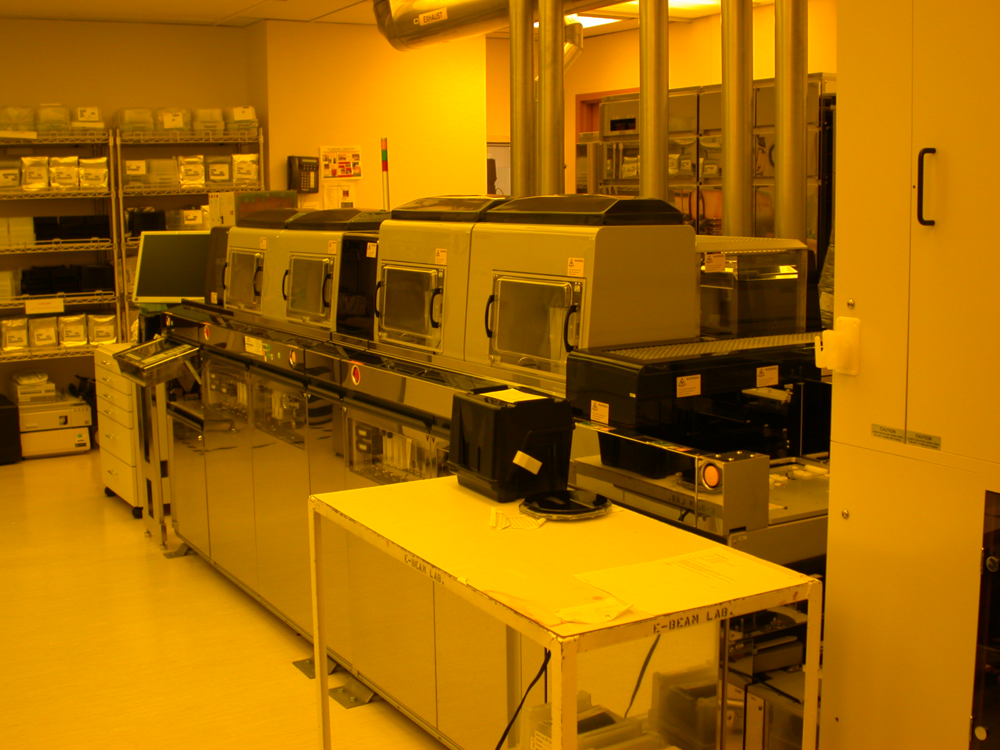
Semiconductor device fabrication is the process used to manufacture semiconductor devices, typically integrated circuits (ICs) such as microprocessors, microcontrollers, and memories (such as Random-access memory, RAM and flash memory). It is a multiple-step Photolithography, photolithographic and physico-chemical process (with steps such as thermal oxidation, thin-film deposition, ion-implantation, etching) during which electronic circuits are gradually created on a wafer (electronics), wafer, typically made of pure single-crystal semiconducting material. Silicon is almost always used, but various compound semiconductors are used for specialized applications. This article focuses on the manufacture of integrated circuits, however steps such as etching and photolithography can be used to manufacture other devices such as LCD and OLED displays. The fabrication process is performed in highly specialized semiconductor fabrication plants, also called foundries or "fabs", with the cen ... [...More Info...] [...Related Items...] OR: [Wikipedia] [Google] [Baidu] |
Intel 4004
The Intel 4004 was part of the 4 chip MCS-4 micro computer set, released by the Intel, Intel Corporation in November 1971; the 4004 being part of the first commercially marketed microprocessor chipset, and the first in a long line of List of Intel processors, Intel central processing units (CPUs). Priced at , the chip marked both a technological and economic milestone in computing. The 4-bit computing, 4-bit 4004 CPU was the first significant commercial example of large-scale integration, showcasing the abilities of the Self-aligned gate, MOS silicon gate technology (SGT). Compared to the existing technology, SGT enabled twice the transistor density and five times the operating speed, making future single-chip CPUs feasible. The MCS-4 chip set design served as a model on how to use SGT for complex logic and memory circuits, accelerating the adoption of SGT by the world's semiconductor industry. The project originated in 1969 when Busicom, Busicom Corp. commissioned Intel to de ... [...More Info...] [...Related Items...] OR: [Wikipedia] [Google] [Baidu] |


