|
Carbon Nanotubes In Interconnects
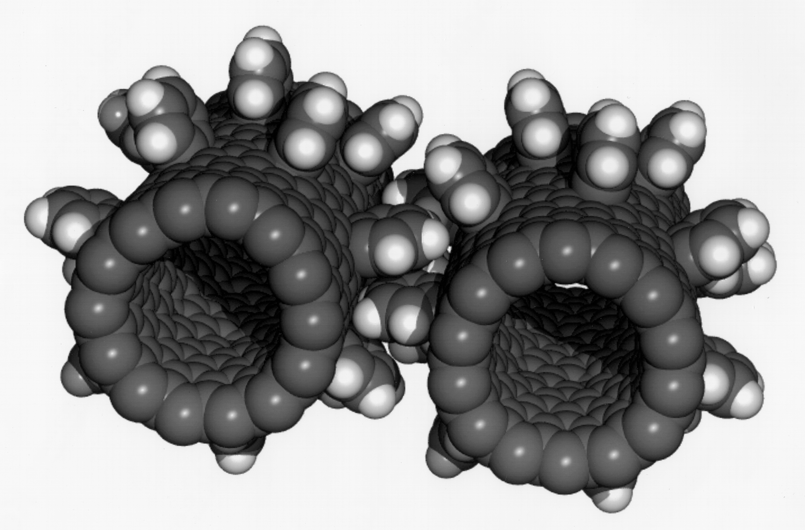
In nanotechnology, carbon nanotube interconnects refer to the proposed use of carbon nanotubes in the interconnects between the elements of an integrated circuit. Carbon nanotubes (CNTs) can be thought of as single atomic layer graphite sheets rolled up to form seamless cylinders. Depending on the direction on which they are rolled, CNTs can be semiconducting or metallic. Metallic carbon nanotubes have been identified as a possible interconnect material for the future technology generations and to replace copper interconnects. Electron transport can go over long nanotube lengths, 1 μm, enabling CNTs to carry very high currents (i.e. up to a current density of 109 A∙ cm−2) with essentially no heating due to nearly one dimensional electronic structure. Despite the current saturation in CNTs at high fields, the mitigation of such effects is possible due to encapsulated nanowires. Carbon nanotubes for interconnects application in Integrated chips have been studied since 2001, ... [...More Info...] [...Related Items...] OR: [Wikipedia] [Google] [Baidu] |
Nanotechnology
Nanotechnology is the manipulation of matter with at least one dimension sized from 1 to 100 nanometers (nm). At this scale, commonly known as the nanoscale, surface area and quantum mechanical effects become important in describing properties of matter. This definition of nanotechnology includes all types of research and technologies that deal with these special properties. It is common to see the plural form "nanotechnologies" as well as "nanoscale technologies" to refer to research and applications whose common trait is scale. An earlier understanding of nanotechnology referred to the particular technological goal of precisely manipulating atoms and molecules for fabricating macroscale products, now referred to as molecular nanotechnology. Nanotechnology defined by scale includes fields of science such as surface science, organic chemistry, molecular biology, semiconductor physics, energy storage, engineering, microfabrication, and molecular engineering. The associated rese ... [...More Info...] [...Related Items...] OR: [Wikipedia] [Google] [Baidu] |
Chemical Vapor Deposition
Chemical vapor deposition (CVD) is a vacuum deposition method used to produce high-quality, and high-performance, solid materials. The process is often used in the semiconductor industry to produce thin films. In typical CVD, the wafer (electronics), wafer (substrate) is exposed to one or more Volatility (chemistry), volatile wikt:precursor, precursors, which chemical reaction, react and/or chemical decomposition, decompose on the substrate surface to produce the desired deposit. Frequently, volatile by-products are also produced, which are removed by gas flow through the reaction chamber. Microfabrication processes widely use CVD to deposit materials in various forms, including: Single crystal, monocrystalline, polycrystalline, amorphous, and Epitaxy, epitaxial. These materials include: silicon (Silicon dioxide, dioxide, silicon carbide, carbide, silicon nitride, nitride, silicon oxynitride, oxynitride), carbon (carbon (fiber), fiber, carbon nanofibers, nanofibers, carbon nanot ... [...More Info...] [...Related Items...] OR: [Wikipedia] [Google] [Baidu] |
Raman Spectroscopy
Raman spectroscopy () (named after physicist C. V. Raman) is a Spectroscopy, spectroscopic technique typically used to determine vibrational modes of molecules, although rotational and other low-frequency modes of systems may also be observed. Raman spectroscopy is commonly used in chemistry to provide a structural fingerprint by which molecules can be identified. Raman spectroscopy relies upon inelastic scattering of photons, known as Raman scattering. A source of monochromatic light, usually from a laser in the visible spectrum, visible, near infrared, or ultraviolet, near ultraviolet range is used, although X-ray Raman scattering, X-rays can also be used. The laser light interacts with molecular vibrations, phonons or other excitations in the system, resulting in the energy of the laser photons being shifted up or down. The shift in energy gives information about the vibrational modes in the system. Time-resolved spectroscopy and infrared spectroscopy typically yields similar y ... [...More Info...] [...Related Items...] OR: [Wikipedia] [Google] [Baidu] |
Electroplating
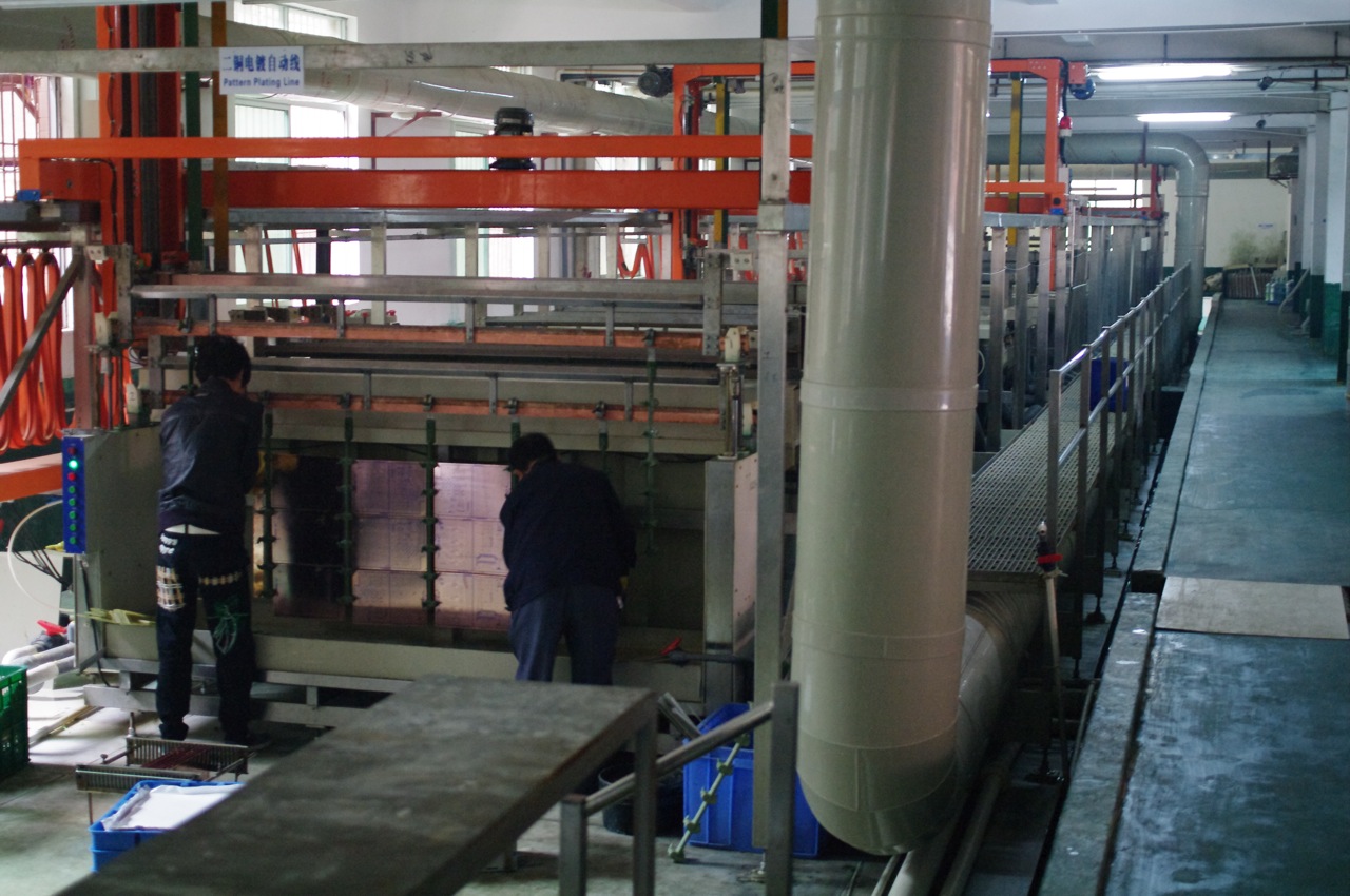
Electroplating, also known as electrochemical deposition or electrodeposition, is a process for producing a metal coating on a solid substrate through the redox, reduction of cations of that metal by means of a direct current, direct electric current. The part to be coated acts as the cathode (negative electrode) of an electrolytic cell; the electrolyte is a solution (chemistry), solution of a salt (chemistry), salt whose cation is the metal to be coated, and the anode (positive electrode) is usually either a block of that metal, or of some inert electrical conductor, conductive material. The current is provided by an external power supply. Electroplating is widely used in industry and decorative arts to improve the surface qualities of objects—such as resistance to abrasion (mechanical), abrasion and corrosion, lubrication, lubricity, reflectivity, electrical conductivity, or appearance. It is used to build up thickness on undersized or worn-out parts and to manufacture metal ... [...More Info...] [...Related Items...] OR: [Wikipedia] [Google] [Baidu] |
CMOS
Complementary metal–oxide–semiconductor (CMOS, pronounced "sea-moss ", , ) is a type of MOSFET, metal–oxide–semiconductor field-effect transistor (MOSFET) semiconductor device fabrication, fabrication process that uses complementary and symmetrical pairs of p-type semiconductor, p-type and n-type semiconductor, n-type MOSFETs for logic functions. CMOS technology is used for constructing integrated circuit (IC) chips, including microprocessors, microcontrollers, memory chips (including Nonvolatile BIOS memory, CMOS BIOS), and other digital logic circuits. CMOS technology is also used for analog circuits such as image sensors (CMOS sensors), data conversion, data converters, RF circuits (RF CMOS), and highly integrated transceivers for many types of communication. In 1948, Bardeen and Brattain patented an insulated-gate transistor (IGFET) with an inversion layer. Bardeen's concept forms the basis of CMOS technology today. The CMOS process was presented by Fairchild Semico ... [...More Info...] [...Related Items...] OR: [Wikipedia] [Google] [Baidu] |
Anode
An anode usually is an electrode of a polarized electrical device through which conventional current enters the device. This contrasts with a cathode, which is usually an electrode of the device through which conventional current leaves the device. A common mnemonic is ACID, for "anode current into device". The direction of conventional current (the flow of positive charges) in a circuit is opposite to the direction of electron flow, so (negatively charged) electrons flow from the anode of a galvanic cell, into an outside or external circuit connected to the cell. For example, the end of a household battery marked with a "+" is the cathode (while discharging). In both a galvanic cell and an electrolytic cell, the anode is the electrode at which the oxidation reaction occurs. In a galvanic cell the anode is the wire or plate having excess negative charge as a result of the oxidation reaction. In an electrolytic cell, the anode is the wire or plate upon which excess positive charge ... [...More Info...] [...Related Items...] OR: [Wikipedia] [Google] [Baidu] |
Thermal Contact
In heat transfer and thermodynamics, a thermodynamic system A thermodynamic system is a body of matter and/or radiation separate from its surroundings that can be studied using the laws of thermodynamics. Thermodynamic systems can be passive and active according to internal processes. According to inter ... is said to be in thermal contact with another system if it can exchange energy through the process of heat. Perfect thermal isolation is an idealization as real systems are always in thermal contact with their environment to some extent. When two solid bodies are in contact, a resistance to heat transfer exists between the bodies. The study of heat conduction between such bodies is called thermal contact conductance (or thermal contact resistance). References See also * Thermal equilibrium - When two objects A and B are in thermal contact and there is no net transfer of thermal energy from A to B or from B to A, they are said to be in thermal equilibrium. The majority ... [...More Info...] [...Related Items...] OR: [Wikipedia] [Google] [Baidu] |
Thermal Conductivity
The thermal conductivity of a material is a measure of its ability to heat conduction, conduct heat. It is commonly denoted by k, \lambda, or \kappa and is measured in W·m−1·K−1. Heat transfer occurs at a lower rate in materials of low thermal conductivity than in materials of high thermal conductivity. For instance, metals typically have high thermal conductivity and are very efficient at conducting heat, while the opposite is true for insulating materials such as mineral wool or Styrofoam. Metals have this high thermal conductivity due to free electrons facilitating heat transfer. Correspondingly, materials of high thermal conductivity are widely used in heat sink applications, and materials of low thermal conductivity are used as thermal insulation. The reciprocal of thermal conductivity is called thermal resistivity. The defining equation for thermal conductivity is \mathbf = - k \nabla T, where \mathbf is the heat flux, k is the thermal conductivity, and \nabla ... [...More Info...] [...Related Items...] OR: [Wikipedia] [Google] [Baidu] |
Ampacity
Ampacity is a portmanteau for ''ampere capacity'', defined by United States National Electrical Codes. Ampacity is defined as the maximum current, in amperes, that a conductor can carry continuously under the conditions of use without exceeding its temperature rating. The ampacity of a conductor depends on its ability to dissipate heat without damage to the conductor or its insulation. This is a function of the insulation temperature rating, the electrical resistance of the conductor material, the ambient temperature, and the ability of the insulated conductor to dissipate heat to the surroundings. All common electrical conductors have some resistance to the flow of electricity. Electric current flowing through conductors heats them. If heat is produced at a sufficient rate, the conductor temperature rises and the insulation can be damaged or ultimately the conductor itself can sag or melt. The ampacity rating for a conductor is based on the conductor diameter, material used ... [...More Info...] [...Related Items...] OR: [Wikipedia] [Google] [Baidu] |
Grain Boundary
In materials science, a grain boundary is the interface between two grains, or crystallites, in a polycrystalline material. Grain boundaries are two-dimensional defects in the crystal structure, and tend to decrease the electrical and thermal conductivity of the material. Most grain boundaries are preferred sites for the onset of corrosion and for the precipitation of new phases from the solid. They are also important to many of the mechanisms of creep. On the other hand, grain boundaries disrupt the motion of dislocations through a material, so reducing crystallite size is a common way to improve mechanical strength, as described by the Hall–Petch relationship. High and low angle boundaries It is convenient to categorize grain boundaries according to the extent of misorientation between the two grains. ''Low-angle grain boundaries'' (''LAGB'') or ''subgrain boundaries'' are those with a misorientation less than about 15 degrees. Generally speaking they are composed of ... [...More Info...] [...Related Items...] OR: [Wikipedia] [Google] [Baidu] |
Electromigration
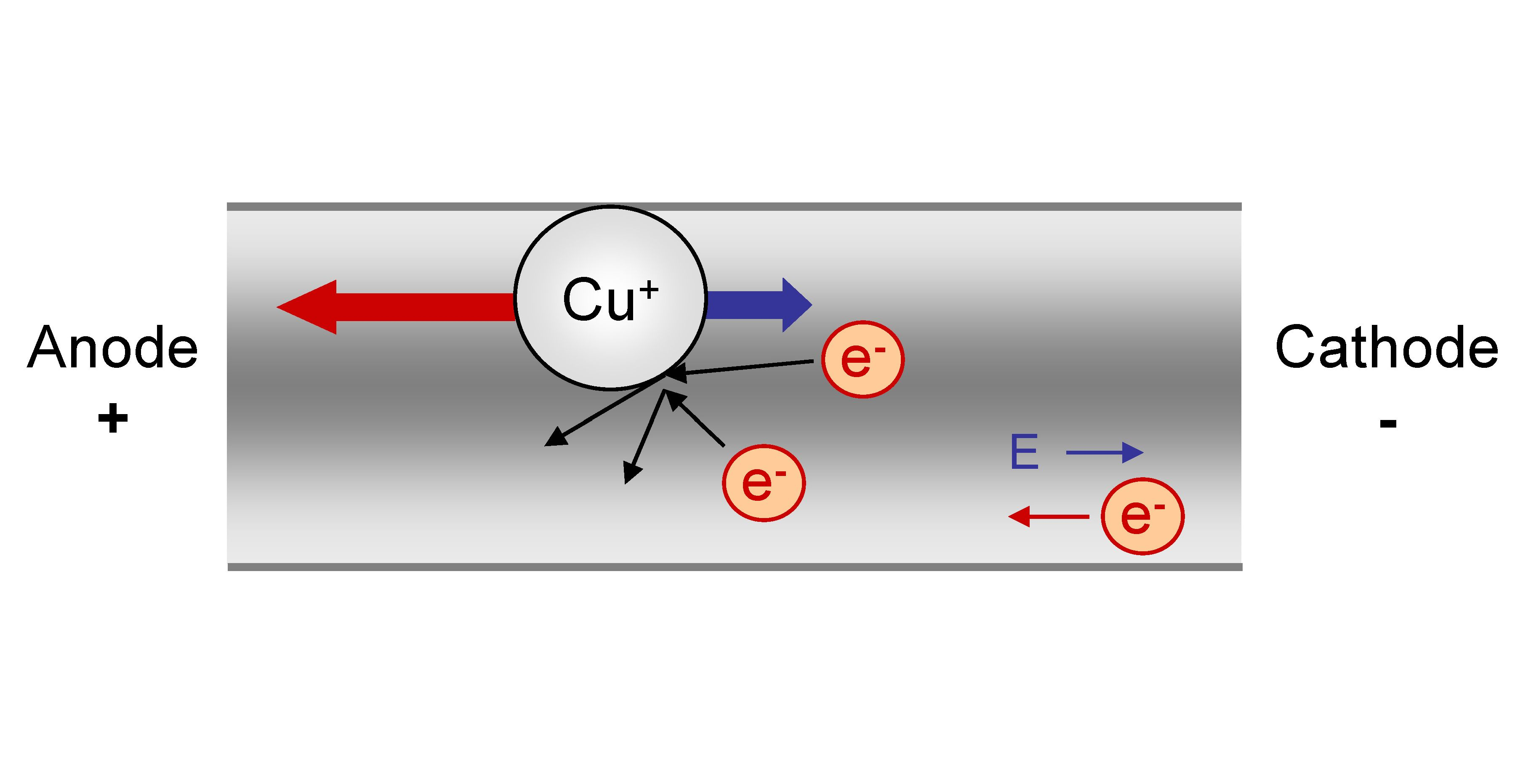
Electromigration is the transport of material caused by the gradual movement of the ions in a Conductor (material), conductor due to the momentum transfer between conducting electrons and diffusing metal atoms. The effect is important in applications where high direct current densities are used, such as in microelectronics and related structures. As the structure size in electronics such as integrated circuits (ICs) decreases, the practical significance of this effect increases. History The phenomenon of electromigration has been known for over 100 years, having been discovered by the French scientist Gerardin. The topic first became of practical interest during the late 1960s when packaged ICs first appeared. The earliest commercially available ICs failed in a mere three weeks of use from runaway electromigration, which led to a major industry effort to correct this problem. The first observation of electromigration in thin films was made by I. Blech.I. Blech: ''Electromigratio ... [...More Info...] [...Related Items...] OR: [Wikipedia] [Google] [Baidu] |
International Technology Roadmap For Semiconductors
The International Technology Roadmap for Semiconductors (ITRS) is a set of documents that was coordinated and organized by Semiconductor Research Corporation and produced by a group of experts in the semiconductor industry. These experts were representative of the sponsoring organisations, including the Semiconductor Industry Associations of Taiwan, South Korea, the United States, Europe, Japan, and China. As of 2017, ITRS is no longer being updated. Its successor is the International Roadmap for Devices and Systems. The documents carried disclaimer: "The ITRS is devised and intended for technology assessment only and is without regard to any commercial considerations pertaining to individual products or equipment". The documents represent best opinion on the directions of research and time-lines up to about 15 years into the future for the following areas of technology: History Constructing an integrated circuit, or any semiconductor device, requires a series of operation ... [...More Info...] [...Related Items...] OR: [Wikipedia] [Google] [Baidu] |


