|
Back Side Grinding
Wafer backgrinding is a semiconductor device fabrication step during which wafer thickness is reduced to allow stacking and high-density packaging of integrated circuits (IC). ICs are produced on semiconductor wafers that undergo a multitude of processing steps. The silicon wafers predominantly used today have diameters of 200 and 300 mm. They are roughly 750 μm thick to ensure a minimum of mechanical stability and to avoid warping during high-temperature processing steps. Smartcards, USB memory sticks, smartphones, handheld music players, and other ultra-compact electronic products would not be feasible in their present form without minimizing the size of their various components along all dimensions. The backside of the wafers are thus ground prior to wafer dicing (separation of the individual microchips). Wafers thinned down to 75 to 50 μm are common today. [...More Info...] [...Related Items...] OR: [Wikipedia] [Google] [Baidu] |
Semiconductor Device Fabrication
Semiconductor device fabrication is the process used to manufacture semiconductor devices, typically integrated circuits (ICs) such as microprocessors, microcontrollers, and memories (such as Random-access memory, RAM and flash memory). It is a multiple-step Photolithography, photolithographic and physico-chemical process (with steps such as thermal oxidation, thin-film deposition, ion-implantation, etching) during which electronic circuits are gradually created on a wafer (electronics), wafer, typically made of pure single-crystal semiconducting material. Silicon is almost always used, but various compound semiconductors are used for specialized applications. This article focuses on the manufacture of integrated circuits, however steps such as etching and photolithography can be used to manufacture other devices such as LCD and OLED displays. The fabrication process is performed in highly specialized semiconductor fabrication plants, also called foundries or "fabs", with the cen ... [...More Info...] [...Related Items...] OR: [Wikipedia] [Google] [Baidu] |
Integrated Circuits
An integrated circuit (IC), also known as a microchip or simply chip, is a set of electronic circuits, consisting of various electronic components (such as transistors, resistors, and capacitors) and their interconnections. These components are etched onto a small, flat piece ("chip") of semiconductor material, usually silicon. Integrated circuits are used in a wide range of electronic devices, including computers, smartphones, and televisions, to perform various functions such as processing and storing information. They have greatly impacted the field of electronics by enabling device miniaturization and enhanced functionality. Integrated circuits are orders of magnitude smaller, faster, and less expensive than those constructed of discrete components, allowing a large transistor count. The IC's mass production capability, reliability, and building-block approach to integrated circuit design have ensured the rapid adoption of standardized ICs in place of designs using discre ... [...More Info...] [...Related Items...] OR: [Wikipedia] [Google] [Baidu] |
Wafer (electronics)
In electronics, a wafer (also called a slice or substrate) is a thin slice of semiconductor, such as a crystalline silicon (c-Si, silicium), used for Semiconductor device fabrication, the fabrication of integrated circuits and, in photovoltaics, to manufacture solar cells. The wafer serves as the substrate (materials science), substrate for microelectronic devices built in and upon the wafer. It undergoes many microfabrication processes, such as doping (semiconductor), doping, ion implantation, Etching (microfabrication), etching, thin-film deposition of various materials, and Photolithography, photolithographic patterning. Finally, the individual microcircuits are separated by wafer dicing and Integrated circuit packaging, packaged as an integrated circuit. History In the semiconductor industry, the term wafer appeared in the 1950s to describe a thin round slice of semiconductor material, typically germanium or silicon. The round shape characteristic of these wafers comes f ... [...More Info...] [...Related Items...] OR: [Wikipedia] [Google] [Baidu] |
Silicon
Silicon is a chemical element; it has symbol Si and atomic number 14. It is a hard, brittle crystalline solid with a blue-grey metallic lustre, and is a tetravalent metalloid (sometimes considered a non-metal) and semiconductor. It is a member of group 14 in the periodic table: carbon is above it; and germanium, tin, lead, and flerovium are below it. It is relatively unreactive. Silicon is a significant element that is essential for several physiological and metabolic processes in plants. Silicon is widely regarded as the predominant semiconductor material due to its versatile applications in various electrical devices such as transistors, solar cells, integrated circuits, and others. These may be due to its significant band gap, expansive optical transmission range, extensive absorption spectrum, surface roughening, and effective anti-reflection coating. Because of its high chemical affinity for oxygen, it was not until 1823 that Jöns Jakob Berzelius was first able to p ... [...More Info...] [...Related Items...] OR: [Wikipedia] [Google] [Baidu] |
Micrometre
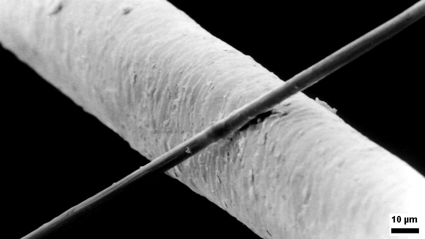
The micrometre (English in the Commonwealth of Nations, Commonwealth English as used by the International Bureau of Weights and Measures; SI symbol: μm) or micrometer (American English), also commonly known by the non-SI term micron, is a unit of length in the International System of Units (SI) equalling (SI standard prefix "micro-" = ); that is, one millionth of a metre (or one thousandth of a millimetre, , or about ). The nearest smaller common SI Unit, SI unit is the nanometre, equivalent to one thousandth of a micrometre, one millionth of a millimetre or one billionth of a metre (). The micrometre is a common unit of measurement for wavelengths of infrared radiation as well as sizes of biological cell (biology), cells and bacteria, and for grading wool by the diameter of the fibres. The width of a single human hair ranges from approximately 20 to . Examples Between 1 μm and 10 μm: * 1–10 μm – length of a typical bacterium * 3–8 μm – width of str ... [...More Info...] [...Related Items...] OR: [Wikipedia] [Google] [Baidu] |
Wafer Dicing
Die singulation, also called wafer dicing, is the process in semiconductor device fabrication by which dies are separated from a finished wafer of semiconductor. It can involve scribing and breaking, mechanical sawing (normally with a machine called a '' dicing saw'') or laser cutting. All methods are typically automated to ensure precision and accuracy. Following the dicing process the individual silicon chips may be encapsulated into chip carriers which are then suitable for use in building electronic devices such as computers, etc. During dicing, wafers are typically mounted on dicing tape which has a sticky backing that holds the wafer on a thin sheet metal frame. Dicing tape has different properties depending on the dicing application. UV curable tapes are used for smaller sizes and non-UV dicing tape for larger die sizes. Dicing saws may use a dicing blade with diamond particles, rotating at 30,000 RPM and cooled with deionized water. Once a wafer has been diced, the p ... [...More Info...] [...Related Items...] OR: [Wikipedia] [Google] [Baidu] |
Purified Water
Purified water is water that has been mechanically filtered or processed to remove impurities and make it suitable for use. Distilled water was, formerly, the most common form of purified water, but, in recent years, water is more frequently purified by other processes including capacitive deionization, reverse osmosis, carbon filtering, microfiltration, ultrafiltration, ultraviolet oxidation, or electrodeionization. Combinations of a number of these processes have come into use to produce ultrapure water of such high purity that its trace contaminants are measured in parts per billion (ppb) or parts per trillion (ppt). Purified water has many uses, largely in the production of medications, in science and engineering laboratories and industries, and is produced in a range of purities. It is also used in the commercial beverage industry as the primary ingredient of any given trademarked bottling formula, in order to maintain product consistency. It can be produced on-site ... [...More Info...] [...Related Items...] OR: [Wikipedia] [Google] [Baidu] |
Die Singulation
Die singulation, also called wafer dicing, is the process in semiconductor device fabrication by which Die (integrated circuit), dies are separated from a finished Wafer (electronics), wafer of semiconductor. It can involve scribing and breaking, mechanical sawing (normally with a machine called a ''dicing saw'') or laser cutting. All methods are typically automated to ensure precision and accuracy. Following the dicing process the individual silicon Integrated circuit, chips may be encapsulated into chip carriers which are then suitable for use in building Electronics, electronic devices such as computers, etc. During dicing, wafers are typically mounted on dicing tape which has a sticky backing that holds the wafer on a thin sheet metal frame. Dicing tape has different properties depending on the dicing application. UV curable tapes are used for smaller sizes and non-UV dicing tape for larger die sizes. Dicing saws may use a dicing blade with diamond particles, rotating at 30,00 ... [...More Info...] [...Related Items...] OR: [Wikipedia] [Google] [Baidu] |
Back-illuminated Sensor
Comparison of simplified back-illuminated and front-illuminated pixel cross-sections A back-illuminated (BI) sensor, also known as back-side illumination (BSI) sensor, is a type of digital image sensor that uses a novel arrangement of the imaging elements to increase the amount of light captured and thereby improve low-light performance. The technique was used for some time in specialized roles like low-light security cameras and astronomy sensors, but was complex to build and required further refinement to become widely used. Sony was the first to reduce these problems and their costs sufficiently to introduce a 5-megapixel 1.75 μm BI CMOS sensor at general consumer prices in 2009.''Sony'', 2009 BI sensors from OmniVision Technologies have since been used in consumer electronics from other manufacturers as in the HTC EVO 4G Android smartphone, and as a major selling point for the camera in Apple's iPhone 4.''Apple'', 2010 Description A traditional, front-illuminated di ... [...More Info...] [...Related Items...] OR: [Wikipedia] [Google] [Baidu] |


