|
Antenna Effect
The antenna effect, more formally plasma induced gate oxide damage, is an effect that can potentially cause yield and reliability problems during the manufacture of MOS integrated circuits. Factories (''fabs'') normally supply antenna rules, which are rules that must be obeyed to avoid this problem. A violation of such rules is called an antenna violation. The word antenna is something of a misnomer in this context—the problem is really the collection of charge, not the normal meaning of antenna, which is a device for converting electromagnetic fields to/from electrical currents. Occasionally the phrase ''antenna effect'' is used in this context, but this is less common since there are many effects,From the above reference: ''Several major antenna effects are considered, like impedance matching, antenna gain, frequency-dependent radiation patterns, and antenna temporal dispersion in the presence of the radio channel.'' and the phrase does not make clear which is meant. Fig ... [...More Info...] [...Related Items...] OR: [Wikipedia] [Google] [Baidu] |
Semiconductor Device Fabrication
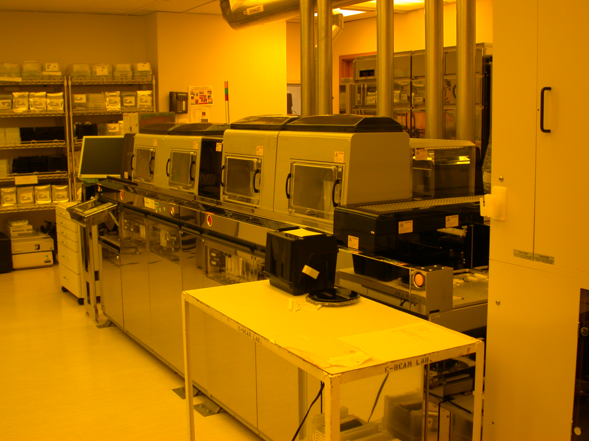
Semiconductor device fabrication is the process used to manufacture semiconductor devices, typically integrated circuits (ICs) such as microprocessors, microcontrollers, and memories (such as Random-access memory, RAM and flash memory). It is a multiple-step Photolithography, photolithographic and physico-chemical process (with steps such as thermal oxidation, thin-film deposition, ion-implantation, etching) during which electronic circuits are gradually created on a wafer (electronics), wafer, typically made of pure single-crystal semiconducting material. Silicon is almost always used, but various compound semiconductors are used for specialized applications. This article focuses on the manufacture of integrated circuits, however steps such as etching and photolithography can be used to manufacture other devices such as LCD and OLED displays. The fabrication process is performed in highly specialized semiconductor fabrication plants, also called foundries or "fabs", with the cen ... [...More Info...] [...Related Items...] OR: [Wikipedia] [Google] [Baidu] |
Antenna (radio)
In radio-frequency engineering, an antenna (American English) or aerial (British English) is an electronic device that converts an alternating current, alternating electric current into radio waves (transmitting), or radio waves into an electric current (receiving). It is the interface between radio waves Radio propagation, propagating through space and electric currents moving in metal Electrical conductor, conductors, used with a transmitter or receiver (radio), receiver. In transmission (telecommunications), transmission, a radio transmitter supplies an electric current to the antenna's Terminal (electronics), terminals, and the antenna radiates the energy from the current as electromagnetic radiation, electromagnetic waves (radio waves). In receiver (radio), reception, an antenna intercepts some of the power of a radio wave in order to produce an electric current at its terminals, that is applied to a receiver to be amplifier, amplified. Antennas are essential components ... [...More Info...] [...Related Items...] OR: [Wikipedia] [Google] [Baidu] |
Integrated Circuit
An integrated circuit (IC), also known as a microchip or simply chip, is a set of electronic circuits, consisting of various electronic components (such as transistors, resistors, and capacitors) and their interconnections. These components are etched onto a small, flat piece ("chip") of semiconductor material, usually silicon. Integrated circuits are used in a wide range of electronic devices, including computers, smartphones, and televisions, to perform various functions such as processing and storing information. They have greatly impacted the field of electronics by enabling device miniaturization and enhanced functionality. Integrated circuits are orders of magnitude smaller, faster, and less expensive than those constructed of discrete components, allowing a large transistor count. The IC's mass production capability, reliability, and building-block approach to integrated circuit design have ensured the rapid adoption of standardized ICs in place of designs using discre ... [...More Info...] [...Related Items...] OR: [Wikipedia] [Google] [Baidu] |
Gate Oxide
The gate oxide is the dielectric layer that separates the metal gate, gate terminal of a MOSFET (metal–oxide–semiconductor field-effect transistor) from the underlying source and drain terminals as well as the conductive channel that connects source and drain when the transistor is turned on. Gate oxide is formed by thermal oxidation of the silicon of the channel to form a thin (5 - 200 nm) insulating layer of silicon dioxide. The insulating silicon dioxide layer is formed through a process of self-limiting oxidation, which is described by the Deal–Grove model. A conductive gate material is subsequently deposited over the gate oxide to form the transistor. The gate oxide serves as the dielectric layer so that the gate can sustain as high as 1 to 5 MV/cm transverse electric field in order to strongly modulate the electrical conductance, conductance of the channel. Above the gate oxide is a thin electrode layer made of a electrical conductor, conductor which can be aluminium ... [...More Info...] [...Related Items...] OR: [Wikipedia] [Google] [Baidu] |
Silicon Dioxide
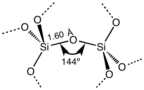
Silicon dioxide, also known as silica, is an oxide of silicon with the chemical formula , commonly found in nature as quartz. In many parts of the world, silica is the major constituent of sand. Silica is one of the most complex and abundant families of materials, existing as a compound of several minerals and as a synthetic product. Examples include fused quartz, fumed silica, opal, and aerogels. It is used in structural materials, microelectronics, and as components in the food and pharmaceutical industries. All forms are white or colorless, although impure samples can be colored. Silicon dioxide is a common fundamental constituent of glass. Structure In the majority of silicon dioxides, the silicon atom shows tetrahedral coordination, with four oxygen atoms surrounding a central Si atomsee 3-D Unit Cell. Thus, SiO2 forms 3-dimensional network solids in which each silicon atom is covalently bonded in a tetrahedral manner to 4 oxygen atoms. In contrast, CO2 is a li ... [...More Info...] [...Related Items...] OR: [Wikipedia] [Google] [Baidu] |
High-κ Dielectric
In the semiconductor industry, the term high-κ dielectric refers to a material with a high dielectric constant (κ, kappa), as compared to silicon dioxide. High-κ dielectrics are used in semiconductor manufacturing processes where they are usually used to replace a silicon dioxide gate dielectric or another dielectric layer of a device. The implementation of high-κ gate dielectrics is one of several strategies developed to allow further miniaturization of microelectronic components, colloquially referred to as extending Moore's Law. Sometimes these materials are called "high-k" (pronounced "high kay"), instead of "high-κ" (high kappa). Need for high-κ materials Silicon dioxide () has been used as a gate oxide material for decades. As metal–oxide–semiconductor field-effect transistors (MOSFETs) have decreased in size, the thickness of the silicon dioxide gate dielectric has steadily decreased to increase the gate capacitance (per unit area) and thereby drive current (per ... [...More Info...] [...Related Items...] OR: [Wikipedia] [Google] [Baidu] |
Lateral Mosfet
Lateral is a geometric term of location which may also refer to: Biology and healthcare * Lateral (anatomy), a term of location meaning "towards the side" * Lateral cricoarytenoid muscle, an intrinsic muscle of the larynx * Lateral release (surgery), a surgical procedure to release tight capsular structures Other uses * ''Lateral'', a digital journal and production of the Cultural Studies Association * ''Lateral'', a podcast by English YouTuber and web developer Tom Scott * Lateral canal, a canal built along the same right-of-way as an existing stream * Lateral consonant, a consonant in which the airstream proceeds along one or both of the sides of the tongue * Lateral mark, a sea mark used in maritime pilotage to indicate the edge of a channel * Lateral modes, an aspect of dynamic stability and control in the field of aircraft flight dynamics * Lateral pass, a non-advancing move in gridiron football * Lateral release (phonetics), the release of a plosive consonant into a lat ... [...More Info...] [...Related Items...] OR: [Wikipedia] [Google] [Baidu] |
Diode
A diode is a two-Terminal (electronics), terminal electronic component that conducts electric current primarily in One-way traffic, one direction (asymmetric electrical conductance, conductance). It has low (ideally zero) Electrical resistance and conductance, resistance in one direction and high (ideally infinite) resistance in the other. A semiconductor diode, the most commonly used type today, is a Crystallinity, crystalline piece of semiconductor material with a p–n junction connected to two electrical terminals. It has an Exponential function, exponential current–voltage characteristic. Semiconductor diodes were the first Semiconductor device, semiconductor electronic devices. The discovery of asymmetric electrical conduction across the contact between a Crystal, crystalline mineral and a metal was made by German physicist Ferdinand Braun in 1874. Today, most diodes are made of silicon, but other semiconducting materials such as gallium arsenide and germanium are also ... [...More Info...] [...Related Items...] OR: [Wikipedia] [Google] [Baidu] |
Reactive-ion Etching
Reactive-ion etching (RIE) is an etching (microfabrication), etching technology used in microfabrication. RIE is a type of dry etching which has different characteristics than Isotropic etching, wet etching. RIE uses chemical reaction, chemically reactive plasma (physics), plasma to remove material deposited on wafer (electronics), wafers. The plasma is generated under low pressure (vacuum) by an electromagnetic field. High-energy ions from the plasma attack the wafer surface and react with it. Equipment A typical (parallel plate) RIE system consists of a cylindrical vacuum chamber, with a wafer (electronics), wafer platter situated in the bottom portion of the chamber. The wafer platter is electrically isolated from the rest of the chamber. Gas enters through small inlets in the top of the chamber, and exits to the vacuum pump system through the bottom. The types and amount of gas used vary depending upon the etch process; for instance, sulfur hexafluoride is commonly used for ... [...More Info...] [...Related Items...] OR: [Wikipedia] [Google] [Baidu] |
Routing (EDA)
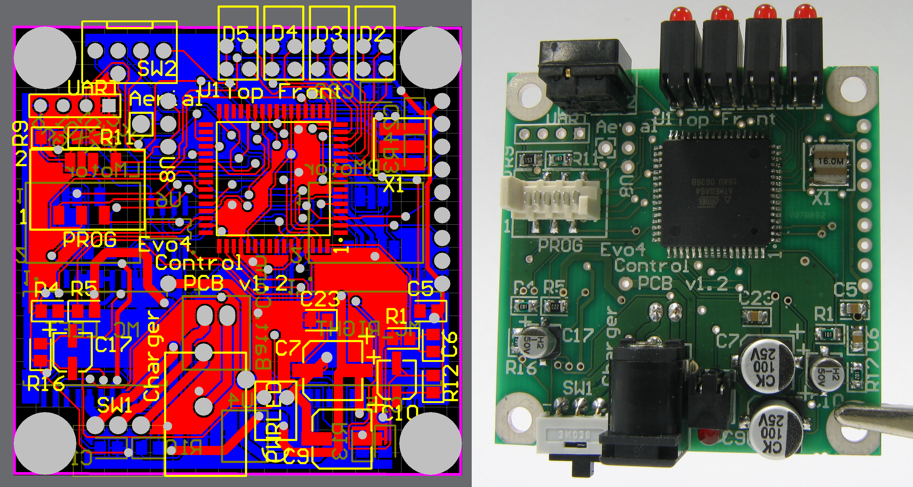
In electronic design, wire routing, commonly called simply routing, is a step in the design of printed circuit boards (PCBs) and integrated circuits (ICs). It builds on a preceding step, called placement (electronic design automation), placement, which determines the location of each active element of an IC or component on a PCB. After placement, the routing step adds wires needed to properly connect the placed components while obeying all design rules for the IC. Together, the placement and routing steps of IC design are known as place and route. The task of all routers is the same. They are given some pre-existing polygons consisting of pin (electronics), pins (also called terminals) on cells, and optionally some pre-existing wiring called preroutes. Each of these polygons are associated with a net (electronics), net, usually by name or number. The primary task of the router is to create geometries such that all terminals assigned to the same net are connected, no terminals a ... [...More Info...] [...Related Items...] OR: [Wikipedia] [Google] [Baidu] |


