|
3 Nm
In semiconductor manufacturing, the 3 nm process is the next die shrink after the 5 nm MOSFET (metal–oxide–semiconductor field-effect transistor) technology node. South Korean chipmaker Samsung started shipping its 3 nm gate all around (GAA) process, named 3GAA, in mid-2022. On 29 December 2022, Taiwanese chip manufacturer TSMC announced that volume production using its 3 nm semiconductor node (N3) was underway with good yields. An enhanced 3 nm chip process called "N3E" may have started production in 2023. American manufacturer Intel planned to start 3 nm production in 2023. Samsung's 3 nm process is based on GAAFET (gate-all-around field-effect transistor) technology, a type of multi-gate MOSFET technology, while TSMC's 3 nm process still uses FinFET (fin field-effect transistor) technology, despite TSMC developing GAAFET transistors. Specifically, Samsung plans to use its own variant of GAAFET called MBCFET (multi-bridge channel field-ef ... [...More Info...] [...Related Items...] OR: [Wikipedia] [Google] [Baidu] |
Semiconductor Manufacturing
Semiconductor device fabrication is the process used to manufacture semiconductor devices, typically integrated circuits (ICs) such as microprocessors, microcontrollers, and memories (such as Random-access memory, RAM and flash memory). It is a multiple-step Photolithography, photolithographic and physico-chemical process (with steps such as thermal oxidation, thin-film deposition, ion-implantation, etching) during which electronic circuits are gradually created on a wafer (electronics), wafer, typically made of pure single-crystal semiconducting material. Silicon is almost always used, but various compound semiconductors are used for specialized applications. This article focuses on the manufacture of integrated circuits, however steps such as etching and photolithography can be used to manufacture other devices such as LCD and OLED displays. The fabrication process is performed in highly specialized semiconductor fabrication plants, also called foundries or "fabs", with the cen ... [...More Info...] [...Related Items...] OR: [Wikipedia] [Google] [Baidu] |
1 Nm Process
In semiconductor manufacturing, the "1 nm process" represents the next significant milestone in MOSFET (metal–oxide–semiconductor field-effect transistor) scaling, succeeding the "2 nm" process node. It continues the industry trend of miniaturization in integrated circuit (IC) technology, which has been essential for improving performance, increasing transistor density, and reducing power consumption. The term "1 nanometer" has no relation to any actual physical feature (such as gate length, metal pitch or gate pitch) of the transistors. According to the projections contained in the 2021 update of the International Roadmap for Devices and Systems published by the Institute of Electrical and Electronics Engineers (IEEE), a "1 nm node range label" is expected to have a contacted gate pitch of 42 nanometers and a tightest metal pitch of 16 nanometers. The first 1 nm chips are expected to be launched in 2027. History In 2008, transistors one atom thick and ten atoms wide were ... [...More Info...] [...Related Items...] OR: [Wikipedia] [Google] [Baidu] |
Extreme Ultraviolet Lithography
Extreme ultraviolet lithography (EUVL, also known simply as EUV) is a technology used in the semiconductor industry for manufacturing integrated circuits (ICs). It is a type of photolithography that uses 13.5 nm extreme ultraviolet (EUV) light from a laser-pulsed tin (Sn) plasma to create intricate patterns on semiconductor substrates. , ASML Holding is the only company that produces and sells EUV systems for chip production, targeting 5 nanometer (nm) and 3 nm process nodes. The EUV wavelengths that are used in EUVL are near 13.5 nanometers (nm), using a laser-pulsed tin (Sn) droplet plasma to produce a pattern by using a reflective photomask to expose a substrate covered by photoresist. Tin ions in the ionic states from Sn IX to Sn XIV give photon emission spectral peaks around 13.5 nm from 4p64d''n'' – 4p54d''n''+1 + 4d''n''−14f ionic state transitions. History and economic impact In the 1960s, visible light was used for the production of integ ... [...More Info...] [...Related Items...] OR: [Wikipedia] [Google] [Baidu] |
Cadence Design Systems
Cadence Design Systems, Inc. (stylized as cādence)Investor's Business DailCEO Lip-Bu Tan Molds Troubled Cadence Into Long-Term LeaderRetrieved November 12, 2020 is an American multinational corporation, multinational technology and computational software company. Headquartered in San Jose, California, Cadence was formed in 1988 through the merger of SDA Systems and ECAD, Inc., ECAD. Initially specialized in Electronic design automation, electronic design automation (EDA) software for the semiconductor industry, currently the company makes software and Electronic hardware, hardware for designing products such as integrated circuits, System on chip, systems on chips (SoCs), printed circuit boards,The StreeHow Cadence Designs the FutureRetrieved July 21, 2020 and pharmaceutical drugs, also licensing intellectual property for the electronics, aerospace, defense and automotive industries, among others. History 1983–1999 Founded in 1983 in San Jose, California, Cadence Design Systems ... [...More Info...] [...Related Items...] OR: [Wikipedia] [Google] [Baidu] |
IMEC
Interuniversity Microelectronics Centre (IMEC; officially stylised as imec) is an international Research and development, research & development organization, active in the fields of nanoelectronics and Digital electronics, digital technologies with headquarters in Belgium. Luc Van den hove has served as president and CEO since 2009. IMEC has more than 5,500 employees and researchers for advanced semiconductor R&D activities, also including system scaling, silicon photonics, artificial intelligence, beyond 5G communications and sensing technologies. In 2022, IMEC's revenue (P&L) totaled 846 million euro. Overview IMEC employs more than 5,500 researchers from more than 90 countries; it has numerous facilities dedicated to research and development around the world, including 12,000 square meters of cleanroom capacity for semiconductor processing. The IMEC headquarters are located in Leuven. History In 1982, the Flemish Government set up a program to strengthen the microelectro ... [...More Info...] [...Related Items...] OR: [Wikipedia] [Google] [Baidu] |
Tainan Science Park
Tainan Science Park () of Taiwan is located in Sinshih, Shanhua and Anding Districts of Tainan City with a total area of , and is a part of the Southern Taiwan Science Park (STSP). History On 1 July 1993, the Executive Yuan approved the establishment of a science park in southern Taiwan as part of the Economic Revitalization Plan. The Phase I site of the park was approved in May 1995 and totaled , marking the beginning of high-tech development in southern Taiwan. Phase II was approved in September 2001 and covered an area of The park focuses on optoelectronics, integrated circuits, biotechnology, and precision machinery industries. See also * Kaohsiung Science Park *Hsinchu Science Park The Hsinchu Science Park (HSP; ) is an industrial park complex that originated as one campus straddled Hsinchu City, Hsinchu County, Chunan and Tongluo, later expanded to cover six campuses across Taiwan. It was established by the government of ... References Further reading * * ... [...More Info...] [...Related Items...] OR: [Wikipedia] [Google] [Baidu] |
EE Times
''EE Times'' (''Electronic Engineering Times'') is an electronics industry magazine published in the United States since 1972. EE Times is currently owned by AspenCore, a division of Arrow Electronics since August 2016. Ownership and status ''EE Times'' was launched in 1972 by Gerard G. Leeds of CMP Publications Inc. In 1999, the Leeds family sold CMP to United Business Media for $900 million. After 2000, ''EE Times'' moved more into web publishing. The shift in advertising from print to online began to accelerate in 2007, and the periodical shed staff to adjust to the downturn in revenue. In July 2013, the digital edition migrated to UBM TechWeb's DeusM community platform. On June 3, 2016, UBM announced that ''EE Times'', along with the rest of its electronics media portfolio ( EDN, Embedded.com, TechOnline, and Datasheets.com), was being sold to AspenCore Media, a company owned by Arrow Electronics, for $23.5 million. The acquisition was completed on August 1, 2016. A ... [...More Info...] [...Related Items...] OR: [Wikipedia] [Google] [Baidu] |
Semiconductor Fabrication Plant
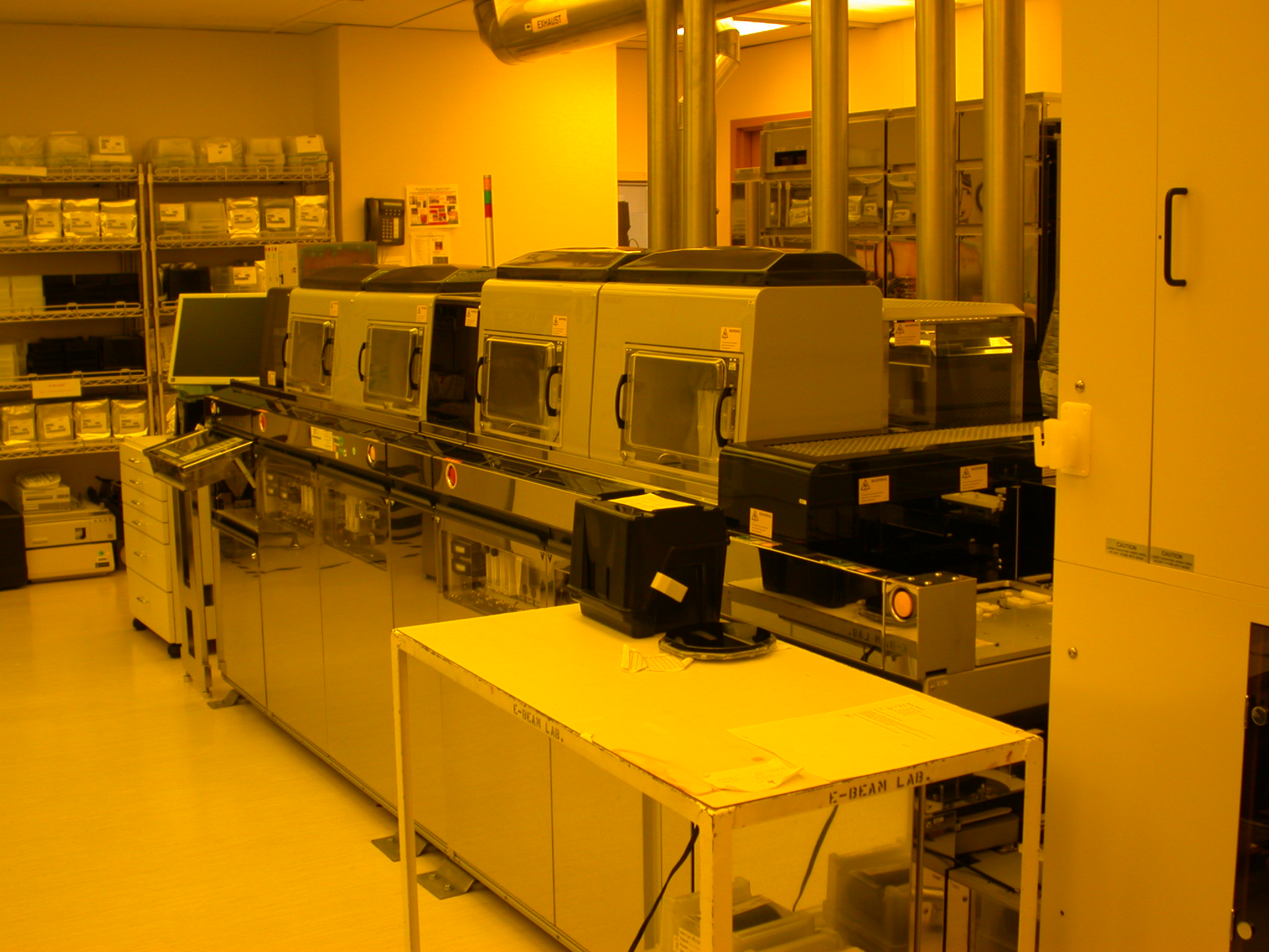
In the microelectronics industry, a semiconductor fabrication plant, also called a ''fab'' or a ''foundry'', is a factory where integrated circuits (ICs) are manufactured. The ''cleanroom'' is where all fabrication takes place and contains the machinery for integrated circuit production such as steppers and/or scanners for photolithography, etching, cleaning, and doping. All these devices are extremely precise and thus extremely expensive. Prices for pieces of equipment for the processing of 300 mm wafers range to upwards of $4,000,000 each with a few pieces of equipment reaching as high as $340,000,000 (e.g. EUV scanners). A typical fab will have several hundred equipment items. Semiconductor fabrication requires many expensive devices. Estimates put the cost of building a new fab at over one billion U.S. dollars with values as high as $3–4 billion not being uncommon. For example, TSMC invested $9.3 billion in its ''Fab15'' in Taiwan. The same company estimations ... [...More Info...] [...Related Items...] OR: [Wikipedia] [Google] [Baidu] |
Nanoelectronic
Nanoelectronics refers to the use of nanotechnology in electronic components. The term covers a diverse set of devices and materials, with the common characteristic that they are so small that inter-atomic interactions and quantum mechanical properties need to be studied extensively. Some of these candidates include: hybrid molecular/semiconductor electronics, one-dimensional nanotubes/nanowires (e.g. carbon nanotube or silicon nanowires) or advanced molecular electronics. Nanoelectronic devices have critical dimensions with a size range between 1 nm and 100 nm. Recent silicon MOSFET (metal–oxide–semiconductor field-effect transistor, or MOS transistor) technology generations are already within this regime, including 22 nanometers CMOS (complementary MOS) nodes and succeeding 14 nm, 10 nm and 7 nm FinFET (fin field-effect transistor) generations. Nanoelectronics is sometimes considered as disruptive technology because present candidates are significantly diffe ... [...More Info...] [...Related Items...] OR: [Wikipedia] [Google] [Baidu] |
Multi-gate
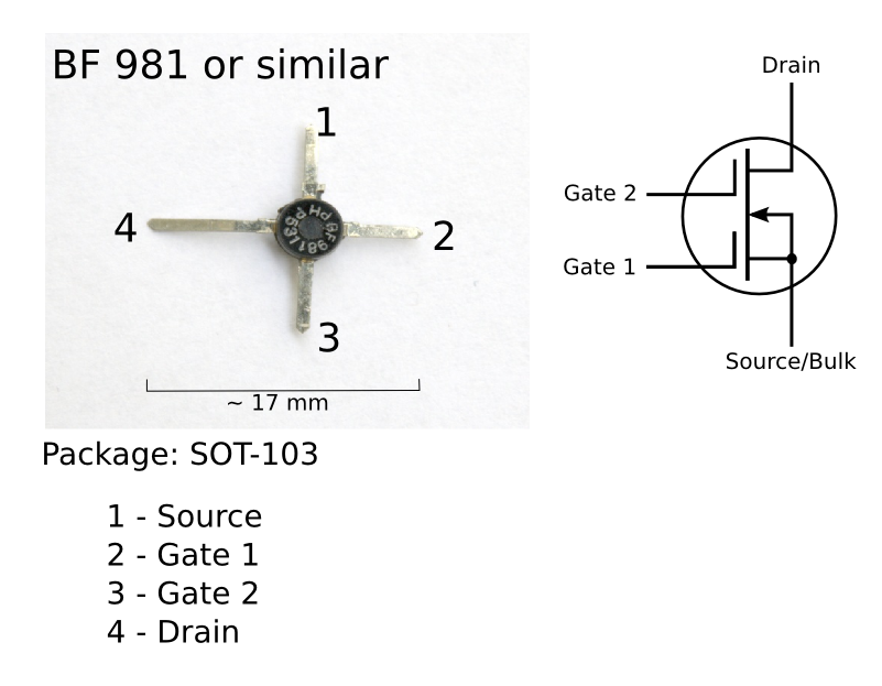
A multigate device, multi-gate MOSFET or multi-gate field-effect transistor (MuGFET) refers to a metal–oxide–semiconductor field-effect transistor (MOSFET) that has more than one gate on a single transistor. The multiple gates may be controlled by a single gate electrode, wherein the multiple gate surfaces act electrically as a single gate, or by independent gate electrodes. A multigate device employing independent gate electrodes is sometimes called a multiple-independent-gate field-effect transistor (MIGFET). The most widely used multi-gate devices are the FinFET (fin field-effect transistor) and the GAAFET (gate-all-around field-effect transistor), which are non-planar transistors, or 3D transistors. Multi-gate transistors are one of the several strategies being developed by MOS semiconductor manufacturers to create ever-smaller microprocessors and memory cells, colloquially referred to as extending Moore's law (in its narrow, specific version concerning density scaling ... [...More Info...] [...Related Items...] OR: [Wikipedia] [Google] [Baidu] |
KAIST
KAIST (originally the Korea Advanced Institute of Science and Technology) is a national university, national research university located in Daedeok Innopolis, Daejeon, South Korea. KAIST was established by the Korean government in 1971 as the nation's first public, research-oriented science and engineering institution. KAIST has been internationally accredited in business education, and hosts the Secretariat of the Association of Asia-Pacific Business Schools (AAPBS). KAIST has 10,504 full-time students and 1,342 faculty researchers (as of the Fall 2019 Semester) and had a total budget of US$765 million in 2013, of which US$459 million was from research contracts. In 2007, KAIST partnered with international institutions and adopted dual degree programs for its students. Its partner institutions include the Technical University of Denmark, Carnegie Mellon University, the Georgia Institute of Technology, Technische Universität Berlin, and the Technical University of Munich. Hi ... [...More Info...] [...Related Items...] OR: [Wikipedia] [Google] [Baidu] |
NMOS Logic
NMOS or nMOS logic (from N-type metal–oxide–semiconductor) uses n-type (-) MOSFETs (metal–oxide–semiconductor field-effect transistors) to implement logic gates and other digital circuits. NMOS transistors operate by creating an inversion layer in a p-type transistor body. This inversion layer, called the n-channel, can conduct electrons between n-type ''source'' and ''drain'' terminals. The n-channel is created by applying voltage to the third terminal, called the ''gate''. Like other MOSFETs, nMOS transistors have four modes of operation: cut-off (or subthreshold), triode, saturation (sometimes called active), and velocity saturation. NMOS AND-by-default logic can produce unusual glitches or buggy behavior in NMOS components, such as the 6502 "illegal opcodes" which are absent in CMOS 6502s. In some cases such as Commodore's VIC-II chip, the bugs present in the chip's logic were extensively exploited by programmers for graphics effects. For many years, NMOS ci ... [...More Info...] [...Related Items...] OR: [Wikipedia] [Google] [Baidu] |


