|
William Shockley
William Bradford Shockley Jr. (February 13, 1910 – August 12, 1989) was an American physicist and inventor. He was the manager of a research group at Bell Labs that included John Bardeen and Walter Brattain. The three scientists were jointly awarded the 1956 Nobel Prize in Physics for "their researches on semiconductors and their discovery of the transistor effect". Partly as a result of Shockley's attempts to commercialize a new transistor design in the 1950s and 1960s, California's Silicon Valley became a hotbed of electronics innovation. In his later life, while a professor of electrical engineering at Stanford University and afterward, Shockley became widely known for his racist views and advocacy of eugenics. Early life and education Shockley was born to American parents in London on February 13, 1910, and was raised in his family's hometown of Palo Alto, California, from the age of three. His father, William Hillman Shockley, was a mining engineer who speculated i ... [...More Info...] [...Related Items...] OR: [Wikipedia] [Google] [Baidu] |
Field-effect Transistor
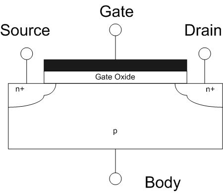
The field-effect transistor (FET) is a type of transistor that uses an electric field to control the flow of current in a semiconductor. FETs ( JFETs or MOSFETs) are devices with three terminals: ''source'', ''gate'', and ''drain''. FETs control the flow of current by the application of a voltage to the gate, which in turn alters the conductivity between the drain and source. FETs are also known as unipolar transistors since they involve single-carrier-type operation. That is, FETs use either electrons (n-channel) or holes (p-channel) as charge carriers in their operation, but not both. Many different types of field effect transistors exist. Field effect transistors generally display very high input impedance at low frequencies. The most widely used field-effect transistor is the MOSFET (metal-oxide-semiconductor field-effect transistor). History The concept of a field-effect transistor (FET) was first patented by Austro-Hungarian physicist Julius Edgar Lilienfeld in ... [...More Info...] [...Related Items...] OR: [Wikipedia] [Google] [Baidu] |
Carrier Generation And Recombination
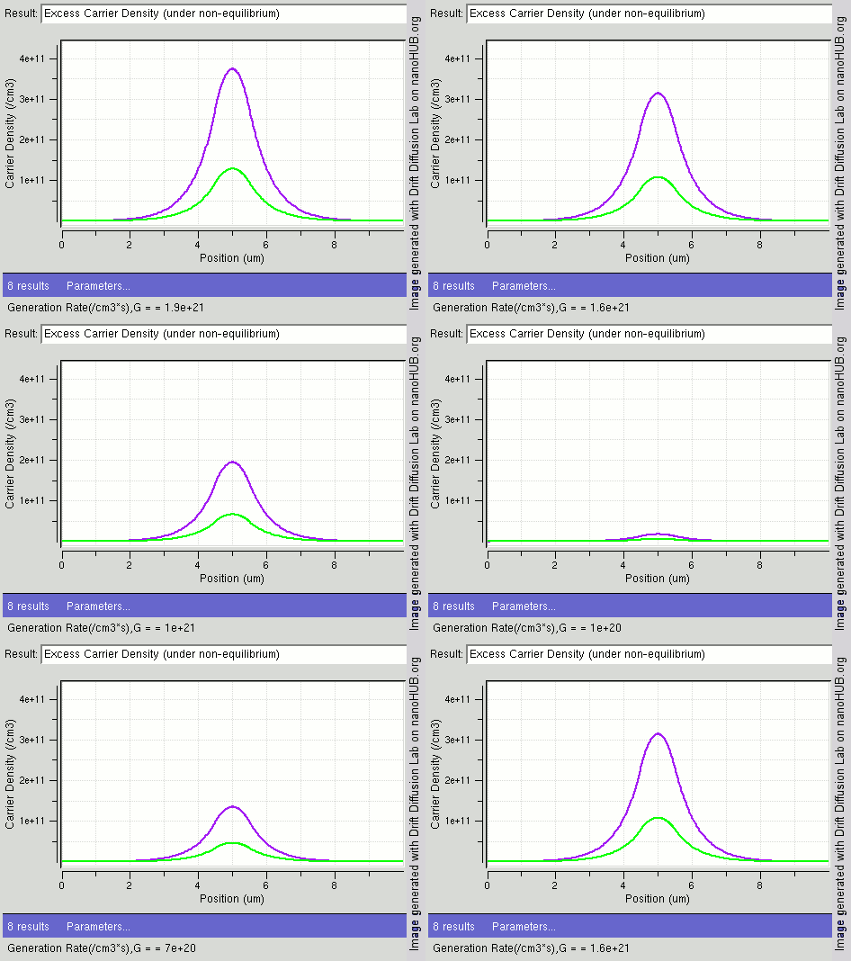
In the solid-state physics of semiconductors, carrier generation and carrier recombination are processes by which mobile charge carriers (electrons and electron holes) are created and eliminated. Carrier generation and recombination processes are fundamental to the operation of many optoelectronic semiconductor devices, such as photodiodes, light-emitting diodes and laser diodes. They are also critical to a full analysis of p-n junction devices such as bipolar junction transistors and p-n junction diodes. The electron–hole pair is the fundamental unit of generation and recombination in inorganic semiconductors, corresponding to an electron transitioning between the valence band and the conduction band where generation of electron is a transition from the valence band to the conduction band and recombination leads to a reverse transition. Overview Like other solids, semiconductor materials have an electronic band structure determined by the crystal properties of the material ... [...More Info...] [...Related Items...] OR: [Wikipedia] [Google] [Baidu] |
Shockley Diode Equation
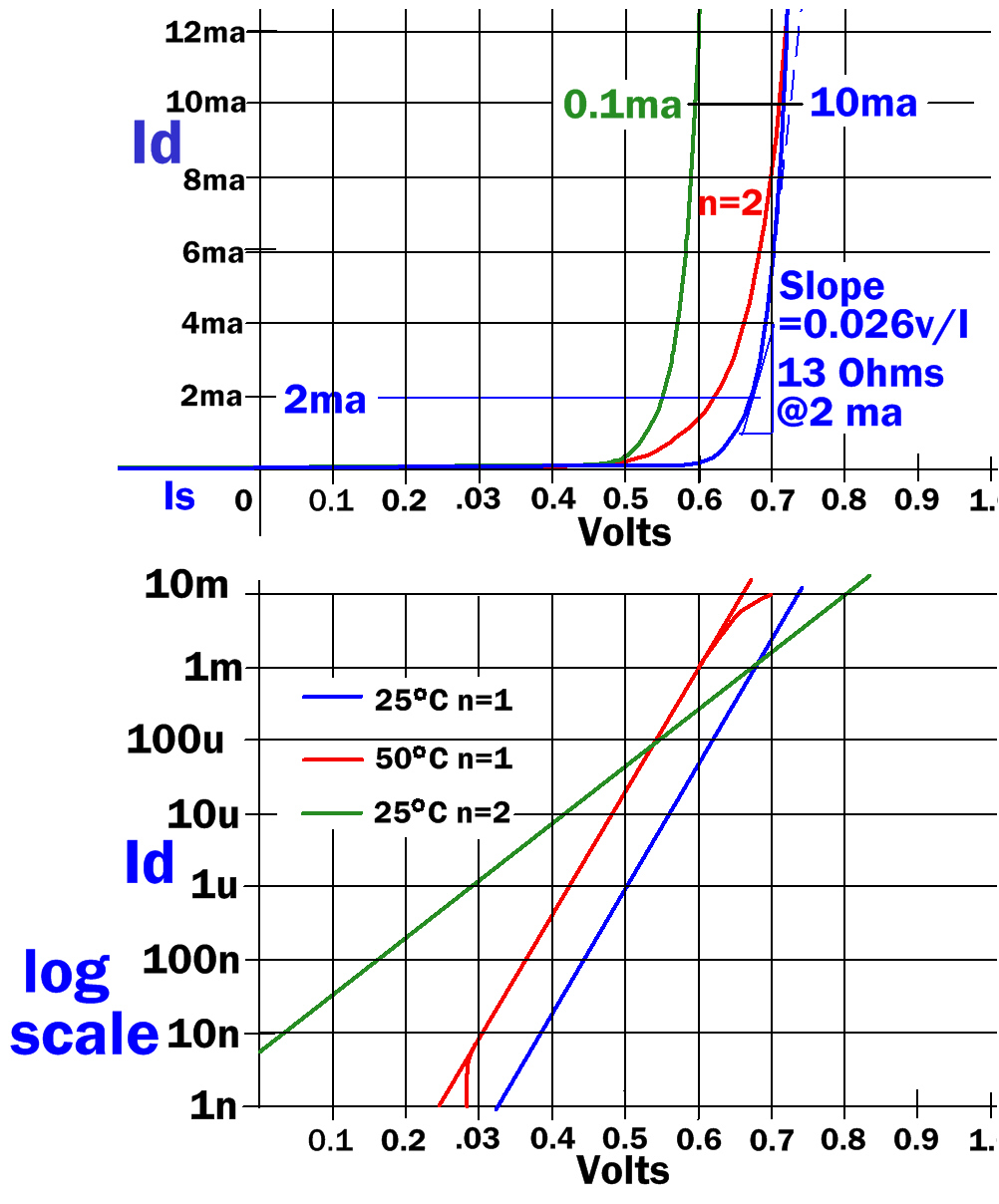
The ''Shockley diode equation'' or the ''diode law'', named after transistor co-inventor William Shockley of Bell Telephone Laboratories, gives the I–V (current-voltage) characteristic of an idealized diode in either forward or reverse bias (applied voltage): :I=I_\mathrm \left( e^\frac - 1 \right) where :''I'' is the diode current, :''I''S is the reverse bias saturation current (or scale current), :''V''D is the voltage across the diode, :''V''T is the thermal voltage ''kT''/''q'' (Boltzmann constant times temperature divided by electron charge), and :''n'' is the ''ideality factor'', also known as the ''quality factor'' or sometimes ''emission coefficient''. The equation is called the ''Shockley ideal diode equation'' when ''n'', the ideality factor, is set equal to 1. The ideality factor ''n'' typically varies from 1 to 2 (though can in some cases be higher), depending on the fabrication process and semiconductor material and is set equal to 1 for the case of an "ideal" diod ... [...More Info...] [...Related Items...] OR: [Wikipedia] [Google] [Baidu] |
Transmission Line Measurement
The Transfer Length Method or the "Transmission Line Model" (both abbreviated as TLM) is a technique used in semiconductor physics and engineering to determine the specific contact resistivity between a metal and a semiconductor. TLM has been developed because with the ongoing device shrinkage in microelectronics the relative contribution of the contact resistance at metal-semiconductor interfaces in a device could not be neglected any more and an accurate measurement method for determining the specific contact resistivity was required. General description The goal of the transfer length method (TLM) is the determination of the specific contact resistivity \rho_C of a metal-semiconductor junction. To create a metal-semiconductor junction a metal film is deposited on the surface of a semiconductor substrate. The TLM is usually used to determine the specific contact resistivity when the metal-semiconductor junction shows ohmic behaviour. In this case the contact resistivity \rho_C ... [...More Info...] [...Related Items...] OR: [Wikipedia] [Google] [Baidu] |
Through-silicon Via
In electronic engineering, a through-silicon via (TSV) or through-chip via is a vertical electrical connection (via) that passes completely through a silicon wafer or die. TSVs are high-performance interconnect techniques used as an alternative to wire-bond and flip chips to create 3D packages and 3D integrated circuits. Compared to alternatives such as package-on-package, the interconnect and device density is substantially higher, and the length of the connections becomes shorter. Classification Dictated by the manufacturing process, there exist three different types of TSVs: ''via-first TSVs'' are fabricated before the individual component (transistors, capacitors, resistors, etc.) are patterned (front end of line, FEOL), ''via-middle TSVs'' are fabricated after the individual component are patterned but before the metal layers ( back-end-of-line, BEOL), and ''via-last TSVs'' are fabricated after (or during) the BEOL process. Via-middle TSVs are currently a popular option ... [...More Info...] [...Related Items...] OR: [Wikipedia] [Google] [Baidu] |
Low-level Injection
Low-level injection conditions for a p–n junction, in physics and electronics, refers to the state where the number of minority carriers generated is small compared to the majority carriers of the material. The semiconductor's majority-carrier concentration will remain (relatively) unchanged, while the minority-carrier concentration sees a large increase. In this condition minority-carrier recombination rates are linear. The following equation must be satisfied for a semiconductor under carrier injection conditions: :n = \Delta n + n_0, where n is the number of electrons, \Delta n is the excess carriers injected into the semiconductor, and n_0 is the equilibrium concentration of electrons in the semiconductor The following relation must also be true, because for every electron injected a hole must also be created to keep a balance of charge: :\Delta n = \Delta p. The assumption of low-level injection can be made regarding an n-type semiconductor, which affects the equations i ... [...More Info...] [...Related Items...] OR: [Wikipedia] [Google] [Baidu] |
Ion Implantation
Ion implantation is a low-temperature process by which ions of one element are accelerated into a solid target, thereby changing the physical, chemical, or electrical properties of the target. Ion implantation is used in semiconductor device fabrication and in metal finishing, as well as in materials science research. The ions can alter the elemental composition of the target (if the ions differ in composition from the target) if they stop and remain in the target. Ion implantation also causes chemical and physical changes when the ions impinge on the target at high energy. The crystal structure of the target can be damaged or even destroyed by the energetic collision cascades, and ions of sufficiently high energy (10s of MeV) can cause nuclear transmutation. General principle Ion implantation equipment typically consists of an ion source, where ions of the desired element are produced, an accelerator, where the ions are electrostatically accelerated to a high energy, an ... [...More Info...] [...Related Items...] OR: [Wikipedia] [Google] [Baidu] |
Process Variation (semiconductor)
Process variation is the naturally occurring variation in the attributes of transistors (length, widths, oxide thickness) when integrated circuits are fabricated. The amount of process variation becomes particularly pronounced at smaller process nodes (<65 nm) as the variation becomes a larger percentage of the full length or width of the device and as feature sizes approach the fundamental dimensions such as the size of atoms and the wavelength of usable light for patterning lithography masks. Process variation causes measurable and predictable variance in the output performance of all circuits but particularly s due to mismatch. If the variance causes the measured or simulated performance of a particular output metric (bandwidth, gain, rise time, etc.) to fall below or rise above the specification for the particular circuit or device, it ... [...More Info...] [...Related Items...] OR: [Wikipedia] [Google] [Baidu] |
Channel Length Modulation
Channel length modulation (CLM) is an effect in field effect transistors, a shortening of the length of the inverted channel region with increase in drain bias for large drain biases. The result of CLM is an increase in current with drain bias and a reduction of output resistance. It is one of several short-channel effects in MOSFET scaling. It also causes distortion in JFET amplifiers. To understand the effect, first the notion of pinch-off of the channel is introduced. The channel is formed by attraction of carriers to the gate, and the current drawn through the channel is nearly a constant independent of drain voltage in saturation mode. However, near the drain, the gate ''and drain'' jointly determine the electric field pattern. Instead of flowing in a channel, beyond the pinch-off point the carriers flow in a subsurface pattern made possible because the drain and the gate both control the current. In the figure at the right, the channel is indicated by a dashed line and b ... [...More Info...] [...Related Items...] OR: [Wikipedia] [Google] [Baidu] |
Hot Electron Injection
Hot or the acronym HOT may refer to: Food and drink *Pungency, in food, a spicy or hot quality *Hot, a wine tasting descriptor Places * Hot district, a district of Chiang Mai province, Thailand **Hot subdistrict, a sub-district of Hot District, Thailand **Tha Kham, Chiang Mai, also known as Hot, a town in Hot District, Chiang Mai province, Thailand *Hot, Albania, a village in the Malësi e Madhe municipality, Shkodër County, Albania Music *H.O.T. pronounced "H. O. T.", (High-Five of Teenagers), a South Korean boy band *Hawaii Opera Theatre, an opera company in Honolulu, Hawaii * Hot (American vocal group), best known for 1977 hit "Angel in Your Arms" 1976–1980 *Hot 97, branding for hip-hop radio station WQHT in New York City Albums * ''Hot'' (Freda Payne album), 1979 * ''Hot'' (Half Japanese album), 1995 * ''Hot'' (Inna album) or the title song (see below), 2009 * ''Hot'' (James Brown album) or the title song (see below), 1976 * ''Hot'' (Mel B album), 2000 * ''Hot'' (Paul ... [...More Info...] [...Related Items...] OR: [Wikipedia] [Google] [Baidu] |
Empty Lattice Approximation
The empty lattice approximation is a theoretical electronic band structure model in which the potential is ''periodic'' and ''weak'' (close to constant). One may also consider an empty irregular lattice, in which the potential is not even periodic.Physics Lecture Notes. P.Dirac, Feynman,R.,1968. Internet, Amazon,25.03.2014. The empty lattice approximation describes a number of properties of energy dispersion relations of non-interacting free electrons that move through a crystal lattice. The energy of the electrons in the "empty lattice" is the same as the energy of free electrons. The model is useful because it clearly illustrates a number of the sometimes very complex features of energy dispersion relations in solids which are fundamental to all electronic band structures. __TOC__ Scattering and periodicity The periodic potential of the lattice in this free electron model must be weak because otherwise the electrons wouldn't be free. The strength of the scattering mainly depe ... [...More Info...] [...Related Items...] OR: [Wikipedia] [Google] [Baidu] |


