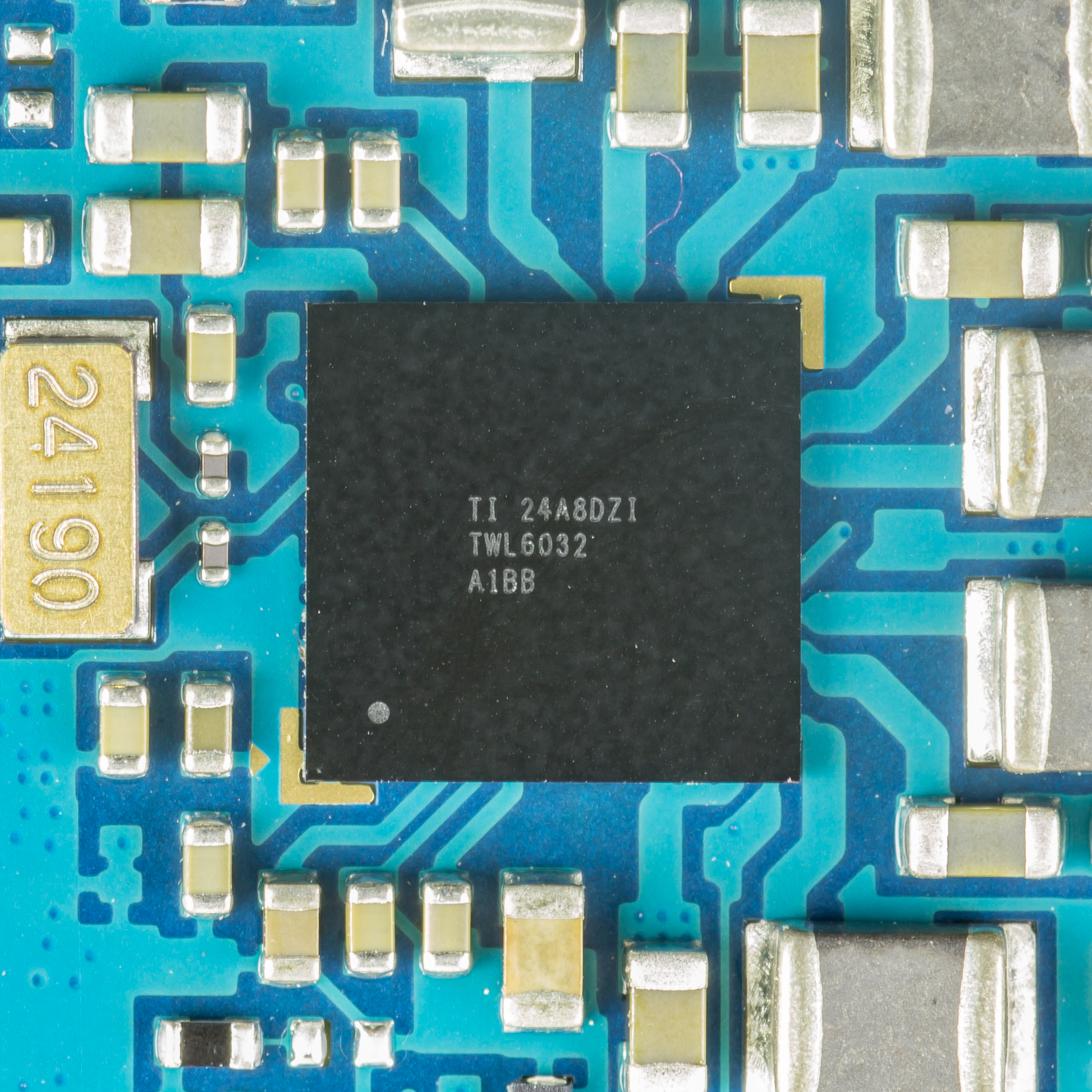
Wafer-level packaging on:
[Wikipedia]
[Google]
[Amazon]
 Wafer-level packaging (WLP) is a process in integrated circuit manufacturing where
 Wafer-level packaging (WLP) is a process in integrated circuit manufacturing where
 packaging
Packaging is the science, art and technology of enclosing or protecting products for distribution, storage, sale, and use. Packaging also refers to the process of designing, evaluating, and producing packages. Packaging can be described as a coo ...
components are attached to an integrated circuit
An integrated circuit (IC), also known as a microchip or simply chip, is a set of electronic circuits, consisting of various electronic components (such as transistors, resistors, and capacitors) and their interconnections. These components a ...
(IC) ''before'' the wafer – on which the IC is fabricated – is diced. In WLP, the top and bottom layers of the packaging and the solder bumps are attached to the integrated circuits while they are still in the wafer. This process differs from a conventional process, in which the wafer is sliced into individual circuits (dice) before the packaging components are attached.
WLP is essentially a true chip-scale package
A chip scale package or chip-scale package (CSP) is a type of integrated circuit package.
Originally, CSP was the acronym for ''chip-size packaging.'' Since only a few packages are chip size, the meaning of the acronym was adapted to ''chip-scal ...
(CSP) technology, since the resulting package is practically of the same size as the die. Wafer-level packaging allows integration of wafer fab, packaging, test, and burn-in at wafer level in order to streamline the manufacturing process undergone by a device from silicon start to customer shipment. As of 2009, there is no single industry-standard method of wafer-level packaging.
A major application area of WLPs is their use in smartphone
A smartphone is a mobile phone with advanced computing capabilities. It typically has a touchscreen interface, allowing users to access a wide range of applications and services, such as web browsing, email, and social media, as well as multi ...
s due to the size constraints. For example, the Apple iPhone 5 has at least eleven different WLPs, the Samsung Galaxy S3 has six WLPs and the HTC One X has seven. Functions provided WLPs in smartphones include sensors, power management, and wireless. The iPhone 7 was rumored to use fan-out wafer-level packaging
Fan-out wafer-level packaging (also known as wafer-level fan-out packaging, fan-out WLP, FOWL packaging, FO-WLP, FOWLP, etc.) is an integrated circuit packaging technology, and an enhancement of standard wafer-level packaging, wafer-level packagin ...
technology in order to achieve a thinner and lighter model.
Wafer-level chip scale packaging (WL-CSP) is the smallest package currently available on the market and is produced by OSAT (Outsourced Semiconductor Assembly and Test) companies, such as Advanced Semiconductor Engineering (ASE). A WL-CSP or WLCSP package is just a bare die with a redistribution layer
A redistribution layer (RDL) is an extra metal layer on an integrated circuit that makes its Input/output, I/O pads available in other locations of the chip, for better access to the pads where necessary.
When an integrated circuit is manufactured ...
(RDL, interposer
An interposer is an electrical interface routing between one socket or connection and another. The purpose of an interposer is to spread a connection to a wider pitch or to reroute a connection to a different connection.I/O pitch) to rearrange the pins or contacts on the die so that they can be big enough and have sufficient spacing so that they can be handled just like a
Raspberry Pi 2 power crashes when exposed to xenon flash
” February 9, 2015. Retrieved February 5, 2016. Thus, careful consideration concerning exposure to extremely bright light will need to be given with wafer-level packaging.
ball grid array
A ball grid array (BGA) is a type of surface-mount packaging (a chip carrier) used for integrated circuits. BGA packages are used to permanently mount devices such as microprocessors. A BGA can provide more interconnection pins than can be pu ...
(BGA) package. The RDL is often made out of a polyamide or polybenzoxazole with copper plated on its surface.
There are two kinds of wafer level packaging: fan-in and fan-out. Fan-in WLCSP packages have an interposer that is the same size as that of the die, where as fan-out WLCSP packages have an interposer that is larger than the die, similar to conventional BGA packages, the difference being that the interposer is built directly atop the die, instead of the die being attached to it and reflowed using the flip chip method. This is also true in fan-in WLSCP packages. In both cases, the die with its interposer may be covered in encapsulating material such as epoxy
Epoxy is the family of basic components or Curing (chemistry), cured end products of epoxy Resin, resins. Epoxy resins, also known as polyepoxides, are a class of reactive prepolymers and polymers which contain epoxide groups. The epoxide fun ...
. Fan.out packages are used in cases where fan-in packages are not able to provide enough connections at a specified cost.
In February 2015, it was discovered that a WL-CSP chip in the Raspberry Pi 2 had issues with xenon flashes (or any other bright flashes of longwave light), inducing the photoelectric effect
The photoelectric effect is the emission of electrons from a material caused by electromagnetic radiation such as ultraviolet light. Electrons emitted in this manner are called photoelectrons. The phenomenon is studied in condensed matter physi ...
within the chip.By Leon Spencer, ZDNet. �Raspberry Pi 2 power crashes when exposed to xenon flash
” February 9, 2015. Retrieved February 5, 2016. Thus, careful consideration concerning exposure to extremely bright light will need to be given with wafer-level packaging.
See also
*List of electronic component packaging types
Integrated circuits and certain other electronic components are put into protective packages to allow easy handling and assembly onto printed circuit boards and to protect the devices from damage. A very large number of package types exist. So ...
* Chip-scale package
A chip scale package or chip-scale package (CSP) is a type of integrated circuit package.
Originally, CSP was the acronym for ''chip-size packaging.'' Since only a few packages are chip size, the meaning of the acronym was adapted to ''chip-scal ...
* Wafer-scale integration
Wafer-scale integration (WSI) is a system of building very-large integrated circuit (commonly called a "chip") networks from an entire wafer (electronics), silicon wafer to produce a single "super-chip". Combining large size and reduced packaging ...
* Wafer bonding
Wafer bonding is a packaging technology on wafer-level for the fabrication of microelectromechanical systems (MEMS), nanoelectromechanical systems (NEMS), microelectronics
Microelectronics is a subfield of electronics. As the name suggests, ...
References
Further reading
* {{Semiconductor packages Electronics manufacturing Semiconductor technology