Integrated circuit
An integrated circuit (IC), also known as a microchip or simply chip, is a set of electronic circuits, consisting of various electronic components (such as transistors, resistors, and capacitors) and their interconnections. These components a ...
s and certain other
electronic component
An electronic component is any basic discrete electronic device or physical entity part of an electronic system used to affect electrons or their associated fields. Electronic components are mostly industrial products, available in a singula ...
s are put into protective
packages to allow easy handling and assembly onto
printed circuit boards
A printed circuit board (PCB), also called printed wiring board (PWB), is a laminated sandwich structure of conductive and insulating layers, each with a pattern of traces, planes and other features (similar to wires on a flat surface) ...
and to protect the devices from damage. A very large number of package types exist. Some package types have standardized dimensions and tolerances, and are registered with trade industry associations such as
JEDEC
The Joint Electron Device Engineering Council (JEDEC) Solid State Technology Association is a consortium of the semiconductor industry headquartered in Arlington County, Virginia, Arlington, United States. It has over 300 members and is focused ...
and
Pro Electron. Other types are proprietary designations that may be made by only one or two manufacturers.
Integrated circuit packaging
Integrated circuit packaging is the final stage of fabrication (semiconductor), semiconductor device fabrication, in which the die (integrated circuit), die is encapsulated in a supporting case that prevents physical damage and corrosion. The ...
is the last assembly process before testing and shipping devices to customers.
Occasionally specially-processed integrated circuit dies are prepared for direct connections to a substrate without an intermediate header or carrier. In
flip chip systems the IC is connected by solder bumps to a substrate. In beam-lead technology, the metallized pads that would be used for
wire bonding
Wire bonding is a method of making interconnections between an integrated circuit (IC) or other semiconductor device and its packaging during semiconductor device fabrication. Wire bonding can also be used to connect an IC to other electronics ...
connections in a conventional chip are thickened and extended to allow external connections to the circuit. Assemblies using "bare" chips have additional packaging or filling with epoxy to protect the devices from moisture.
Through-hole packages
Through-hole technology uses holes drilled through the
printed circuit board
A printed circuit board (PCB), also called printed wiring board (PWB), is a Lamination, laminated sandwich structure of electrical conduction, conductive and Insulator (electricity), insulating layers, each with a pattern of traces, planes ...
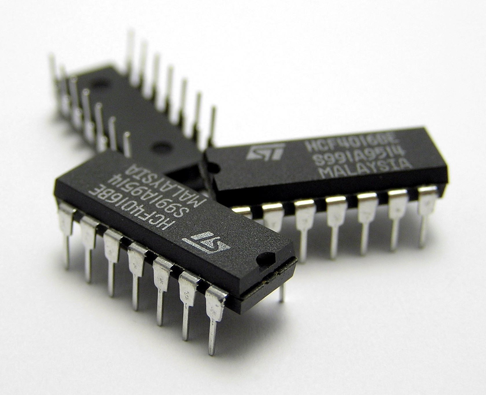
(PCB) for mounting the components. The component has leads that are soldered to pads on the PCB to electrically and mechanically connect them to the PCB.
Surface mount
Chip on board is a packaging technique that directly connects a die to a PCB, without an
interposer or
lead frame.
Chip carrier
A
chip carrier
In electronics, a chip carrier is one of several kinds of surface-mount technology packages for integrated circuits (commonly called "chips"). Connections are made on all four edges of a square package; compared to the internal cavity for mount ...
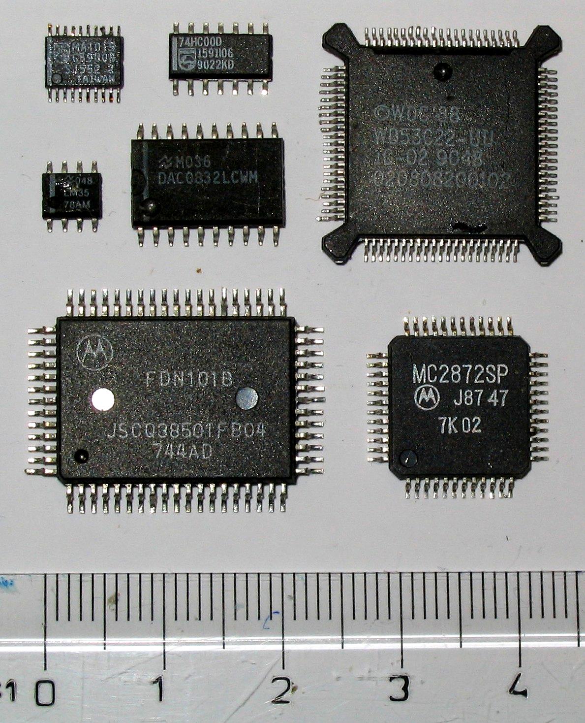
is a rectangular package with contacts on all four edges. Leaded chip carriers have metal leads wrapped around the edge of the package, in the shape of a letter J. Leadless chip carriers have metal pads on the edges. Chip carrier packages may be made of ceramic or plastic and are usually secured to a printed circuit board by soldering, though sockets can be used for testing.
Pin grid arrays
Flat packages
Small outline packages
A small outline integrated circuit (SOIC) is a surface-mounted integrated circuit (IC) package which occupies an area about 30–50% less than an equivalent dual in-line package (DIP), with a typical thickness being 70% less. They are generally available in the same pin-outs as their counterpart DIP ICs.
Chip-scale packages
According to IPC's standard J-STD-012, Implementation of Flip Chip and Chip Scale Technology, in order to qualify as chip scale, the package must have an area no greater than 1.2 times that of the die and it must be a single-die, direct surface mountable package. Another criterion that is often applied to qualify these packages as CSPs is their ball pitch should be no more than 1 mm.
Chip-scale package

Ball grid array
Ball grid array (BGA) uses the underside of the package to place pads with
balls of solder in grid pattern as connections to PCB.
[
]
Transistor, diode, small-pin-count IC packages
* MELF: Metal electrode leadless face (usually for resistors and diodes)
* SOD: Small-outline diode.
* SOT: Small-outline transistor (also SOT-23, SOT-223, SOT-323).
* TO-XX: wide range of small pin count packages often used for discrete parts like transistors or diodes.
** TO-3
In electronics, TO-3 is a designation for a standardized metal semiconductor package used for power semiconductors, including transistors, silicon controlled rectifiers, and, integrated circuits. ''TO'' stands for "Transistor Outline" and relates ...
: Panel-mount with leads
** TO-5: Metal can package with radial leads
** TO-18: Metal can package with radial leads
** TO-39
** TO-46
** TO-66: Similar shape to the TO-3 but smaller
** TO-92
The TO-92 is a widely used style of semiconductor package mainly used for transistors. The case is often made of epoxy or plastic, and offers compact size at a very low cost.
History and origin
The JEDEC TO-92 descriptor is derived from the ori ...
: Plastic-encapsulated package with three leads
** TO-99: Metal can package with eight radial leads
** TO-100: Metal can package with ten radial leads, similar to TO-99
** TO-126: Plastic-encapsulated package with three leads and a hole for mounting on a heat sink
** TO-220: Through-hole plastic package with a (usually) metal heat sink tab and three leads
** TO-226
** TO-247:
Dimension reference
Surface-mount
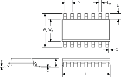 ; C: Clearance between IC body and PCB
; H: Total height
; T: Lead thickness
; L: Total carrier length
; LW: Lead width
; LL: Lead length
; P: Pitch
Through-hole
 ; C: Clearance between IC body and board
; H: Total height
; T: Lead thickness
; L: Total carrier length
; LW: Lead width
; LL: Lead length
; P: Pitch
; WB: IC body width
; WL: Lead-to-lead width
Package dimensions
All measurements below are given in mm. To convert mm to mils, divide mm by 0.0254 (i.e., 2.54 mm / 0.0254 = 100 mil).
; C: Clearance between package body and PCB.
; H: Height of package from pin tip to top of package.
; T: Thickness of pin.
; L: Length of package body only.
; LW: Pin width.
; LL: Pin length from package to pin tip.
; P: Pin pitch (distance between conductors to the PCB).
; WB: Width of the package body only.
; WL: Length from pin tip to pin tip on the opposite side.
Dual row
Quad rows
LGA
Multi-chip packages
A variety of techniques for interconnecting several chips within a single package have been proposed and researched:
* SiP ( system in package)
* PoP (package on package
Package on a package (PoP) is an integrated circuit packaging method to vertically combine ball grid array (BGA) packages for discrete logic and Semiconductor memory, memory. Two or more packages are installed atop each other, i.e. stacked, with a ...
)
* 3D-SICs, Monolithic 3D ICs, and other three-dimensional integrated circuit
A three-dimensional integrated circuit (3D IC) is a MOSFET, MOS (metal-oxide semiconductor) integrated circuit (IC) manufactured by stacking as many as 16 or more ICs and interconnecting them vertically using, for instance, through-silicon vias (TS ...
s
* Multi-chip module
A multi-chip module (MCM) is generically an electronic assembly (such as a package with a number of conductor terminals or Lead (electronics), "pins") where multiple integrated circuits (ICs or "chips"), semiconductor Die (integrated circuit), d ...
* WSI (wafer-scale integration
Wafer-scale integration (WSI) is a system of building very-large integrated circuit (commonly called a "chip") networks from an entire wafer (electronics), silicon wafer to produce a single "super-chip". Combining large size and reduced packaging ...
)
* Proximity communication
By terminal count
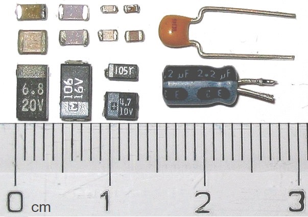 Surface-mount components are usually smaller than their counterparts with leads, and are designed to be handled by machines rather than by humans. The
 electronics industry
The electronics industry is the industry (economics), industry that produces electronic devices. It emerged in the 20th century and is today one of the largest global industries. Contemporary society uses a vast array of electronic devices that ar ...
has standardized package shapes and sizes (the leading standardisation body is JEDEC
The Joint Electron Device Engineering Council (JEDEC) Solid State Technology Association is a consortium of the semiconductor industry headquartered in Arlington County, Virginia, Arlington, United States. It has over 300 members and is focused ...
).
The codes given in the chart below usually tell the length and width of the components in tenths of millimeters or hundredths of inches. For example, a metric 2520 component is 2.5 mm by 2.0 mm which corresponds roughly to 0.10 inches by 0.08 inches (hence, imperial size is 1008). Exceptions occur for imperial in the two smallest rectangular passive sizes. The metric codes still represent the dimensions in mm, even though the imperial size codes are no longer aligned. Problematically, some manufacturers are developing metric 0201 components with dimensions of ,
Two-terminal packages
Rectangular passive components
Mostly resistor
A resistor is a passive two-terminal electronic component that implements electrical resistance as a circuit element. In electronic circuits, resistors are used to reduce current flow, adjust signal levels, to divide voltages, bias active e ...
s and capacitor
In electrical engineering, a capacitor is a device that stores electrical energy by accumulating electric charges on two closely spaced surfaces that are insulated from each other. The capacitor was originally known as the condenser, a term st ...
s.
Tantalum capacitors
Aluminum capacitors
Small-outline diode (SOD)
Metal electrode leadless face (MELF)
Mostly resistor
A resistor is a passive two-terminal electronic component that implements electrical resistance as a circuit element. In electronic circuits, resistors are used to reduce current flow, adjust signal levels, to divide voltages, bias active e ...
s and diode
A diode is a two-Terminal (electronics), terminal electronic component that conducts electric current primarily in One-way traffic, one direction (asymmetric electrical conductance, conductance). It has low (ideally zero) Electrical resistance ...
s; barrel shaped components, dimensions do not match those of rectangular references for identical codes.
DO-214
Commonly used for rectifier, Schottky, and other diodes.
Three- and four-terminal packages
Small-outline transistor (SOT)
Other
*DPAK (TO-252, SOT-428): Discrete Packaging. Developed by Motorola
Motorola, Inc. () was an American multinational telecommunications company based in Schaumburg, Illinois. It was founded by brothers Paul and Joseph Galvin in 1928 and had been named Motorola since 1947. Many of Motorola's products had been ...
to house higher powered devices. Comes in threeD2PAK
The Double Decawatt Package, D2PAK, SOT404 or DDPAK, standardized as TO-263, is a semiconductor package type intended for surface mounting on circuit boards. The TO-263 is designed by Motorola. They are similar to the earlier TO-220-style package ...
(TO-263, SOT-404): Bigger than the DPAK; basically a surface mount equivalent of the TO220 through-hole package. Comes in 3, 5, 6, 7, 8 or 9-terminal versions.
Five- and six-terminal packages
Small-outline transistor (SOT)


Packages with more than six terminals
Dual-in-line
* Flatpack was one of the earliest surface-mounted packages.
* Small-outline integrated circuit (SOIC): dual-in-line, 8 or more pins, gull-wing lead form, pin spacing 1.27 mm.
* Small-outline package, J-leaded (SOJ): The same as SOIC except J-leaded.
Quad-in-line
* Plastic leaded chip carrier (PLCC): square, J-lead, pin spacing 1.27 mm
*Quad flat package ( QFP): various sizes, with pins on all four sides
*Low-profile quad flat-package ( LQFP): 1.4 mm high, varying sized and pins on all four sides
*Plastic quad flat-pack ( PQFP), a square with pins on all four sides, 44 or more pins
*Ceramic quad flat-pack ( CQFP): similar to PQFP
*Metric quad flat-pack ( MQFP): a QFP package with metric pin distribution
*Thin quad flat-pack ( TQFP), a thinner version of LQFP
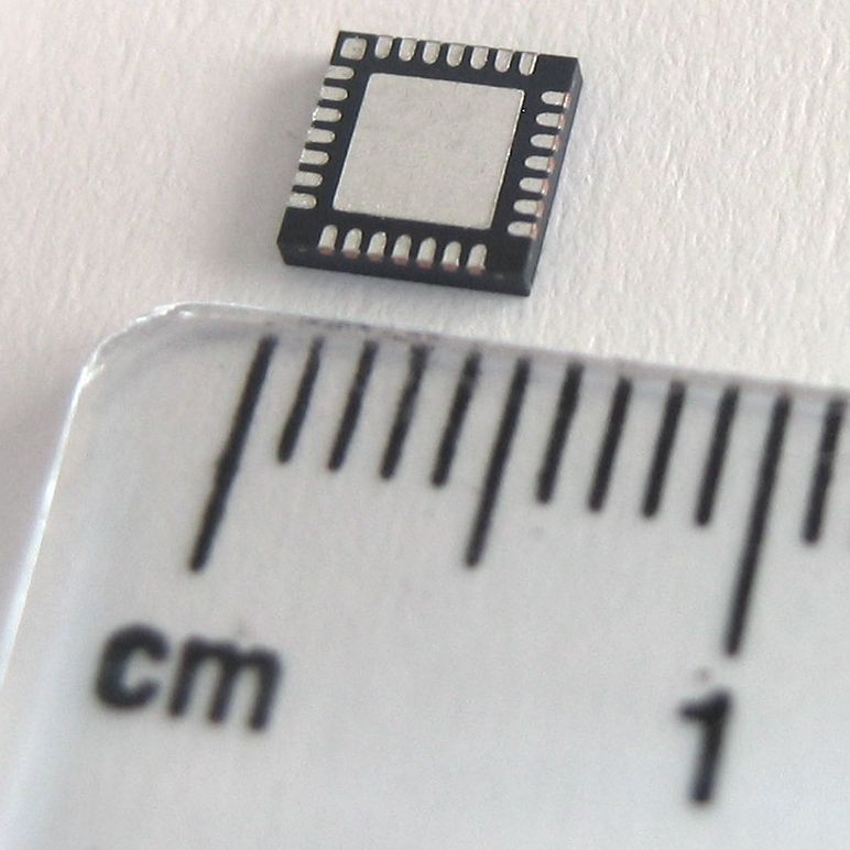
*Quad flat no-lead ( QFN): smaller footprint than leaded equivalent
* Leadless chip carrier (LCC): contacts are recessed vertically to "wick-in" solder. Common in aviation electronics because of robustness to mechanical vibration.
*Micro leadframe package ( MLP, MLF): with a 0.5 mm contact pitch, no leads (same as QFN)
*Power quad flat no-lead ( PQFN): with exposed die-pads for heatsinking
Grid arrays
* Ball grid array
A ball grid array (BGA) is a type of surface-mount packaging (a chip carrier) used for integrated circuits. BGA packages are used to permanently mount devices such as microprocessors. A BGA can provide more interconnection pins than can be pu ...
(BGA): A square or rectangular array of solder balls on one surface, ball spacing typically
** Fine-pitch ball grid array ( FBGA): A square or rectangular array of solder balls on one surface
** Low-profile fine-pitch ball grid array ( LFBGA): A square or rectangular array of solder balls on one surface, ball spacing typically 0.8 mm
** Micro ball grid array ( μBGA): Ball spacing less than 1 mm
** Thin fine-pitch ball grid array ( TFBGA): A square or rectangular array of solder balls on one surface, ball spacing typically 0.5 mm
* Land grid array (LGA): An array of bare lands only. Similar to in appearance to QFN, but mating is by spring pins within a socket rather than solder.
* Column grid array (CGA): A circuit package in which the input and output points are high-temperature solder cylinders or columns arranged in a grid pattern.
** Ceramic column grid array (CCGA): A circuit package in which the input and output points are high-temperature solder cylinders or columns arranged in a grid pattern. The body of the component is ceramic.
* Lead-less package (LLP): A package with metric pin distribution (0.5 mm pitch).
Non-packaged devices
Although surface-mount, these devices require specific process for assembly.
* Chip-on-board (COB), a bare silicon
Silicon is a chemical element; it has symbol Si and atomic number 14. It is a hard, brittle crystalline solid with a blue-grey metallic lustre, and is a tetravalent metalloid (sometimes considered a non-metal) and semiconductor. It is a membe ...
chip, that is usually an integrated circuit, is supplied without a package (which is usually a lead frame overmolded with epoxy
Epoxy is the family of basic components or Curing (chemistry), cured end products of epoxy Resin, resins. Epoxy resins, also known as polyepoxides, are a class of reactive prepolymers and polymers which contain epoxide groups. The epoxide fun ...
) and is attached, often with epoxy, directly to a circuit board. The chip is then wire bonded and protected from mechanical damage and contamination by an epoxy "glob-top".
*Chip-on-flex (COF), a variation of COB, where a chip is mounted directly to a flex circuit. Tape-automated bonding process is also a chip-on-flex process as well.
*Chip-on-glass (COG), a variation of COB, where a chip, typically a liquid crystal display
A liquid-crystal display (LCD) is a flat-panel display or other Electro-optic modulator, electronically modulated optical device that uses the light-modulating properties of liquid crystals combined with polarizers to display information. Liq ...
(LCD) controller, is mounted directly on glass.
*Chip-on-wire (COW), a variation of COB, where a chip, typically a LED or RFID chip, is mounted directly on wire, thus making it a very thin and flexible wire. Such wire may then be covered with cotton, glass or other materials to make into smart textiles or electronic textiles.
There are often subtle variations in package details from manufacturer to manufacturer, and even though standard designations are used, designers need to confirm dimensions when laying out printed circuit boards.
See also
* Surface-mount technology
Surface-mount technology (SMT), originally called planar mounting, is a method in which the electrical components are mounted directly onto the surface of a printed circuit board (PCB). An electrical component mounted in this manner is referred ...
* Three-dimensional integrated circuit
A three-dimensional integrated circuit (3D IC) is a MOSFET, MOS (metal-oxide semiconductor) integrated circuit (IC) manufactured by stacking as many as 16 or more ICs and interconnecting them vertically using, for instance, through-silicon vias (TS ...
* Interposer
* IPC (electronics)
IPC is a global trade association whose aim is to standardize the assembly and production requirements of Electronics, electronic equipment and assemblies. IPC is headquartered in Bannockburn, Illinois, United States with additional offices in W ...
* List of chip carriers
* List of electronics package dimensions
Integrated circuits and certain other electronic components are put into protective semiconductor package, packages to allow easy handling and assembly onto printed circuit boards and to protect the devices from damage. A very large number of pa ...
* Redistribution layer
A redistribution layer (RDL) is an extra metal layer on an integrated circuit that makes its Input/output, I/O pads available in other locations of the chip, for better access to the pads where necessary.
When an integrated circuit is manufactured ...
* Small-outline transistor
* Wafer-level packaging
References
External links
JEDEC JEP95
official list of all (over 500) standard electronic packages
Fairchild Index of Package Information
* ttps://web.archive.org/web/20120418031551/http://www.intersil.com/design/packages/ Intersil packaging information
ICpackage.org
Solder Pad Layout Dimensions
International Microelectronics And Packaging Society
A spreadsheet of semiconductor outline dimensions and names, cross-referencing JEDEC, ProElectron, Soviet and commercial packages, past and present. Updated semi-annually.
An archived web page with links to package drawing collections of SMD, hermetic, plastic, RF, coaxial and hybrid power module varieties.corresponding to dimensions and names listed in the previous spreadsheet pages.
{{DEFAULTSORT:Integrated circuit packaging types
Semiconductor packages
Electronics lists

 ; C: Clearance between IC body and PCB
; H: Total height
; T: Lead thickness
; L: Total carrier length
; LW: Lead width
; LL: Lead length
; P: Pitch
 Surface-mount components are usually smaller than their counterparts with leads, and are designed to be handled by machines rather than by humans. The