|
Phosphosilicate Glass
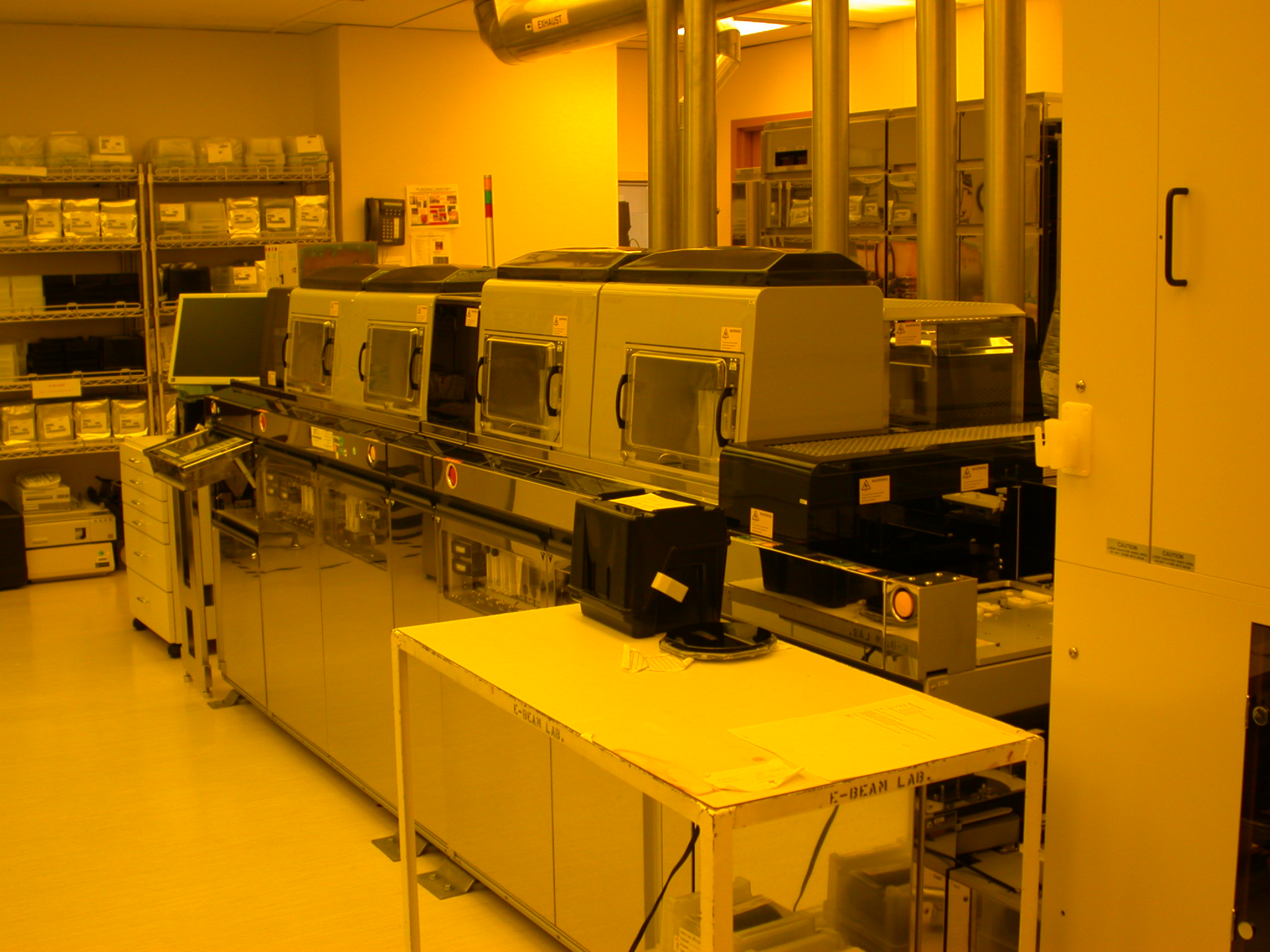
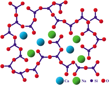
Phosphosilicate glass, commonly referred to by the acronym PSG, is a silicate glass commonly used in semiconductor device fabrication for intermetal layers, i.e., insulating layers deposited between succeedingly higher metal or conducting layers, due to its effect in gettering alkali ions. Another common type of phosphosilicate glass is borophosphosilicate glass (BPSG). Soda-lime phosphosilicate glasses also form the basis for bioactive glasses (e.g. Bioglass), a family of materials which chemically convert to mineralised bone (hydroxy-carbonate-apatite) in physiological fluid. Bismuth doped phosphosilicate glasses are being explored for use as the active gain medium in fiber lasers for fiber-optic communication. See also * Wafer (electronics) In electronics, a wafer (also called a slice or substrate) is a thin slice of semiconductor, such as a crystalline silicon (c-Si, silicium), used for Semiconductor device fabrication, the fabrication of integrated circuits and, in ph ... [...More Info...] [...Related Items...] OR: [Wikipedia] [Google] [Baidu] |
Silicate Glass
Glass is an amorphous ( non-crystalline) solid. Because it is often transparent and chemically inert, glass has found widespread practical, technological, and decorative use in window panes, tableware, and optics. Some common objects made of glass are named after the material, e.g., a "glass" for drinking, "glasses" for vision correction, and a "magnifying glass". Glass is most often formed by rapid cooling (quenching) of the molten form. Some glasses such as volcanic glass are naturally occurring, and obsidian has been used to make arrowheads and knives since the Stone Age. Archaeological evidence suggests glassmaking dates back to at least 3600 BC in Mesopotamia, Egypt, or Syria. The earliest known glass objects were beads, perhaps created accidentally during metalworking or the production of faience, which is a form of pottery using lead glazes. Due to its ease of formability into any shape, glass has been traditionally used for vessels, such as bowls, vases, bottles, ... [...More Info...] [...Related Items...] OR: [Wikipedia] [Google] [Baidu] |
Fabrication (semiconductor)
Semiconductor device fabrication is the process used to manufacture semiconductor devices, typically integrated circuits (ICs) such as microprocessors, microcontrollers, and memories (such as Random-access memory, RAM and flash memory). It is a multiple-step Photolithography, photolithographic and physico-chemical process (with steps such as thermal oxidation, thin-film deposition, ion-implantation, etching) during which electronic circuits are gradually created on a wafer (electronics), wafer, typically made of pure single-crystal semiconducting material. Silicon is almost always used, but various compound semiconductors are used for specialized applications. This article focuses on the manufacture of integrated circuits, however steps such as etching and photolithography can be used to manufacture other devices such as LCD and OLED displays. The fabrication process is performed in highly specialized semiconductor fabrication plants, also called foundries or "fabs", with the cen ... [...More Info...] [...Related Items...] OR: [Wikipedia] [Google] [Baidu] |
Borophosphosilicate Glass
Borophosphosilicate glass, commonly known as BPSG, is a type of silicate glass that includes additives of both boron and phosphorus. Silicate glasses such as PSG and borophosphosilicate glass are commonly used in semiconductor device fabrication for intermetal layers, i.e., insulating layers deposited between succeedingly higher metal or conducting layers. BPSG has been implicated in increasing a device's susceptibility to soft errors since the boron-10 isotope is good at capturing thermal neutrons from cosmic radiation. It then undergoes fission producing a gamma ray, an alpha particle, and a lithium ion. These products may then dump charge into nearby structures, causing data loss (bit flipping, or single event upset). In critical designs, depleted boron consisting almost entirely of boron-11 is used to avoid this effect as a radiation hardening Radiation hardening is the process of making electronic components and circuits resistant to damage or malfunction caused by h ... [...More Info...] [...Related Items...] OR: [Wikipedia] [Google] [Baidu] |
Bioglass
Bioglass 45S5 or calcium sodium phosphosilicate, is a bioactive glass specifically composed of 45 wt% SiO2, 24.5 wt% CaO, 24.5 wt% Na2O, and 6.0 wt% P2O5. Typical applications of Bioglass 45S5 include: bone grafting biomaterials, repair of periodontal defects, cranial and maxillofacial repair, wound care, blood loss control, stimulation of vascular regeneration, and nerve repair. The name "Bioglass" was trademarked by the University of Florida as a name for the original 45S5 composition. It should therefore only be used in reference to the 45S5 composition and not as a general term for bioactive glasses. Bioglass 45S5 is available commercially under the registered trade name NovaMin, which is owned by the pharmaceutical company GlaxoSmithKline. NovaMin is bioactive glass that has been ground into a fine particulate with a median size of less than 20 μm. It can reduce dentin hypersensitivity by blocking open dentinal tubules and by supplying calcium (Ca2+) ... [...More Info...] [...Related Items...] OR: [Wikipedia] [Google] [Baidu] |
Apatite
Apatite is a group of phosphate minerals, usually hydroxyapatite, fluorapatite and chlorapatite, with high concentrations of Hydroxide, OH−, Fluoride, F− and Chloride, Cl− ion, respectively, in the crystal. The formula of the admixture of the three most common Endmember (mineralogy), endmembers is written as Calcium, Ca10(Phosphate, PO4)6(OH,F,Cl)2, and the crystal unit cell formulae of the individual minerals are written as Ca10(PO4)6(OH)2, Ca10(PO4)6F2 and Ca10(PO4)6Cl2. The mineral was named apatite by the German geologist Abraham Gottlob Werner in 1786, although the specific mineral he had described was reclassified as fluorapatite in 1860 by the German mineralogist Karl Friedrich August Rammelsberg. Apatite is often mistaken for other minerals. This tendency is reflected in the mineral's name, which is derived from the Greek word ἀπατάω (apatáō), which means ''to deceive''. Geology Apatite is very common as an accessory mineral in igneous and metamorphic roc ... [...More Info...] [...Related Items...] OR: [Wikipedia] [Google] [Baidu] |
Bismuth
Bismuth is a chemical element; it has symbol Bi and atomic number 83. It is a post-transition metal and one of the pnictogens, with chemical properties resembling its lighter group 15 siblings arsenic and antimony. Elemental bismuth occurs naturally, and its sulfide and oxide forms are important commercial ores. The free element is 86% as dense as lead. It is a brittle metal with a silvery-white color when freshly produced. Surface oxidation generally gives samples of the metal a somewhat rosy cast. Further oxidation under heat can give bismuth a vividly iridescent appearance due to thin-film interference. Bismuth is both the most diamagnetic element and one of the least thermally conductive metals known. Bismuth was formerly understood to be the element with the highest atomic mass whose nuclei do not spontaneously decay. However, in 2003 it was found to be very slightly radioactive. The metal's only primordial isotope, bismuth-209, undergoes alpha decay with a half-l ... [...More Info...] [...Related Items...] OR: [Wikipedia] [Google] [Baidu] |
Dopant
A dopant (also called a doping agent) is a small amount of a substance added to a material to alter its physical properties, such as electrical or optics, optical properties. The amount of dopant is typically very low compared to the material being doped. When doped into crystalline substances, the dopant's atoms get incorporated into the crystal lattice of the substance. The crystalline materials are frequently either crystals of a semiconductor such as silicon and germanium for use in solid-state electronics, or transparency and translucency, transparent crystals for use in the production of various laser types; however, in some cases of the latter, noncrystalline substances such as glass can also be doped with impurities. In solid-state electronics using the proper types and amounts of dopants in semiconductors is what produces the p-type semiconductors and n-type semiconductors that are essential for making transistors and diodes. Transparent crystals Lasing media The p ... [...More Info...] [...Related Items...] OR: [Wikipedia] [Google] [Baidu] |
Active Gain Medium
The active laser medium (also called a gain medium or lasing medium) is the source of optical gain within a laser. The gain results from the stimulated emission of photons through electronic or molecular transitions to a lower energy state from a higher energy state previously populated by a pump source. Examples of active laser media include: * Certain crystals, typically doped with rare-earth ions (e.g. neodymium, ytterbium, or erbium) or transition metal ions (titanium or chromium); most often yttrium aluminium garnet ( Y3 Al5 O12), yttrium orthovanadate (YVO4), or sapphire (Al2O3); and not often caesium cadmium bromide ( Cs Cd Br3) (solid-state lasers) * Glasses, e.g. silicate or phosphate glasses, doped with laser-active ions; * Gases, e.g. mixtures of helium and neon (HeNe), nitrogen, argon, krypton, carbon monoxide, carbon dioxide, or metal vapors; ( gas lasers) * Semiconductors, e.g. gallium arsenide (GaAs), indium gallium arsenide (InGaAs), or gallium nitride (GaN). * ... [...More Info...] [...Related Items...] OR: [Wikipedia] [Google] [Baidu] |
Fiber Laser
A fiber laser (or fibre laser in Commonwealth English) is a laser in which the active gain medium is an optical fiber doped with rare-earth elements such as erbium, ytterbium, neodymium, dysprosium, praseodymium, thulium and holmium. They are related to doped fiber amplifiers, which provide light amplification without lasing. Fiber nonlinearities, such as stimulated Raman scattering or four-wave mixing, can also provide gain and thus serve as gain media for a fiber laser. Characteristics An advantage of fiber lasers over other types of lasers is that the laser light is both generated and delivered by an inherently flexible medium, which allows easier delivery to the focusing location and target. This can be important for laser cutting, welding, and folding of metals and polymers. Another advantage is high output power compared to other types of laser. Fiber lasers can have active regions several kilometers long, and so can provide very high optical gain. They can sup ... [...More Info...] [...Related Items...] OR: [Wikipedia] [Google] [Baidu] |
Fiber-optic Communication
Fiber-optic communication is a form of optical communication for transmitting information from one place to another by sending pulses of infrared or visible light through an optical fiber. The light is a form of carrier wave that is modulated to carry information. Fiber is preferred over electrical cabling when high bandwidth, long distance, or immunity to electromagnetic interference is required. This type of communication can transmit voice, video, and telemetry through local area networks or across long distances. Optical fiber is used by many telecommunications companies to transmit telephone signals, internet communication, and cable television signals. Researchers at Bell Labs have reached a record bandwidth–distance product of over kilometers per second using fiber-optic communication. Background First developed in the 1970s, fiber-optics have revolutionized the telecommunications industry and have played a major role in the advent of the Information Age. ... [...More Info...] [...Related Items...] OR: [Wikipedia] [Google] [Baidu] |
Laser Focus World
''Laser Focus World'' is a monthly magazine published by Endeavor Business Media covering laser, photonics and optoelectronics technologies, applications, and markets. Many qualified professionals in those fields receive it free of charge; it is also possible to subscribe to the magazine. History and profile ''Laser Focus World'' has been published since 1965. Retrieved January 26, 2007 It is published on a monthly basis and owned by Endeavor Business Media. The headquarters of the magazine is in Nashua, New Hampshire
Nashua () is a city in southern New Hampshire, United States. A ...
[...More Info...] [...Related Items...] OR: [Wikipedia] [Google] [Baidu] |
Wafer (electronics)
In electronics, a wafer (also called a slice or substrate) is a thin slice of semiconductor, such as a crystalline silicon (c-Si, silicium), used for Semiconductor device fabrication, the fabrication of integrated circuits and, in photovoltaics, to manufacture solar cells. The wafer serves as the substrate (materials science), substrate for microelectronic devices built in and upon the wafer. It undergoes many microfabrication processes, such as doping (semiconductor), doping, ion implantation, Etching (microfabrication), etching, thin-film deposition of various materials, and Photolithography, photolithographic patterning. Finally, the individual microcircuits are separated by wafer dicing and Integrated circuit packaging, packaged as an integrated circuit. History In the semiconductor industry, the term wafer appeared in the 1950s to describe a thin round slice of semiconductor material, typically germanium or silicon. The round shape characteristic of these wafers comes f ... [...More Info...] [...Related Items...] OR: [Wikipedia] [Google] [Baidu] |


