|
Resist (semiconductor Fabrication)
In semiconductor fabrication, a resist is a thin layer used to transfer a circuit pattern to the semiconductor substrate which it is deposited upon. A resist can be patterned via lithography to form a (sub)micrometer-scale, temporary mask that protects selected areas of the underlying substrate during subsequent processing steps. The material used to prepare said thin layer is typically a viscous solution. Resists are generally proprietary mixtures of a polymer or its precursor and other small molecules (e.g. photoacid generators) that have been specially formulated for a given lithography technology. Resists used during photolithography are called photoresists. Background Semiconductor devices (as of 2005) are built by depositing and patterning many thin layers. The patterning steps, or lithography, define the function of the device and the density of its components. For example, in the ''interconnect layers'' of a modern microprocessor, a conductive material (copper or alumi ... [...More Info...] [...Related Items...] OR: [Wikipedia] [Google] [Baidu] |
Semiconductor Fabrication
Semiconductor device fabrication is the process used to manufacture semiconductor devices, typically integrated circuits (ICs) such as microprocessors, microcontrollers, and memories (such as RAM and flash memory). It is a multiple-step photolithographic and physico-chemical process (with steps such as thermal oxidation, thin-film deposition, ion-implantation, etching) during which electronic circuits are gradually created on a wafer, typically made of pure single-crystal semiconducting material. Silicon is almost always used, but various compound semiconductors are used for specialized applications. This article focuses on the manufacture of integrated circuits, however steps such as etching and photolithography can be used to manufacture other devices such as LCD and OLED displays. The fabrication process is performed in highly specialized semiconductor fabrication plants, also called foundries or "fabs", with the central part being the " clean room". In more advanced semi ... [...More Info...] [...Related Items...] OR: [Wikipedia] [Google] [Baidu] |
Microelectromechanical Systems
MEMS (micro-electromechanical systems) is the technology of microscopic devices incorporating both electronic and moving parts. MEMS are made up of components between 1 and 100 micrometres in size (i.e., 0.001 to 0.1 mm), and MEMS devices generally range in size from 20 micrometres to a millimetre (i.e., 0.02 to 1.0 mm), although components arranged in arrays (e.g., digital micromirror devices) can be more than 1000 mm2. They usually consist of a central unit that processes data (an integrated circuit chip such as microprocessor) and several components that interact with the surroundings (such as microsensors). Because of the large surface area to volume ratio of MEMS, forces produced by ambient electromagnetism (e.g., electrostatic charges and magnetic moments), and fluid dynamics (e.g., surface tension and viscosity) are more important design considerations than with larger scale mechanical devices. MEMS technology is distinguished from molecular nanotechnol ... [...More Info...] [...Related Items...] OR: [Wikipedia] [Google] [Baidu] |
Nanolithography
Nanolithography (NL) is a growing field of techniques within nanotechnology dealing with the engineering (patterning e.g. etching, depositing, writing, printing etc) of Nanometre, nanometer-scale structures on various materials. The modern term reflects on a design of structures built in range of 10−9 to 10−6 meters, i.e. nanometer scale. Essentially, the field is a derivative of lithography, only covering very small structures. All NL methods can be categorized into four groups: photolithography, photo lithography, scanning lithography, soft lithography and other miscellaneous techniques. History Nanolithography has evolved from the need to increase the number of sub-micrometer features (e.g. transistors, capacitors etc.) in an integrated circuit in order to keep up with Moore's law, Moore's Law. While Lithography, lithographic techniques have been around since the late 18th century, none were applied to nanoscale structures until the mid-1950s. With evolution of the semico ... [...More Info...] [...Related Items...] OR: [Wikipedia] [Google] [Baidu] |
Electron Beam Lithography
Electron-beam lithography (often abbreviated as e-beam lithography or EBL) is the practice of scanning a focused beam of electrons to draw custom shapes on a surface covered with an electron-sensitive film called a resist (exposing). The electron beam changes the solubility of the resist, enabling selective removal of either the exposed or non-exposed regions of the resist by immersing it in a solvent (developing). The purpose, as with photolithography, is to create very small structures in the resist that can subsequently be transferred to the substrate material, often by etching. The primary advantage of electron-beam lithography is that it can draw custom patterns (direct-write) with sub-10 nm resolution. This form of maskless lithography has high resolution but low throughput, limiting its usage to photomask fabrication, low-volume production of semiconductor devices, and research and development. Systems Electron-beam lithography systems used in commercial application ... [...More Info...] [...Related Items...] OR: [Wikipedia] [Google] [Baidu] |
Wafer (electronics)
In electronics, a wafer (also called a slice or substrate) is a thin slice of semiconductor, such as a crystalline silicon (c-Si, silicium), used for Semiconductor device fabrication, the fabrication of integrated circuits and, in photovoltaics, to manufacture solar cells. The wafer serves as the substrate (materials science), substrate for microelectronic devices built in and upon the wafer. It undergoes many microfabrication processes, such as doping (semiconductor), doping, ion implantation, Etching (microfabrication), etching, thin-film deposition of various materials, and Photolithography, photolithographic patterning. Finally, the individual microcircuits are separated by wafer dicing and Integrated circuit packaging, packaged as an integrated circuit. History In the semiconductor industry, the term wafer appeared in the 1950s to describe a thin round slice of semiconductor material, typically germanium or silicon. The round shape characteristic of these wafers comes f ... [...More Info...] [...Related Items...] OR: [Wikipedia] [Google] [Baidu] |
Spin Coating
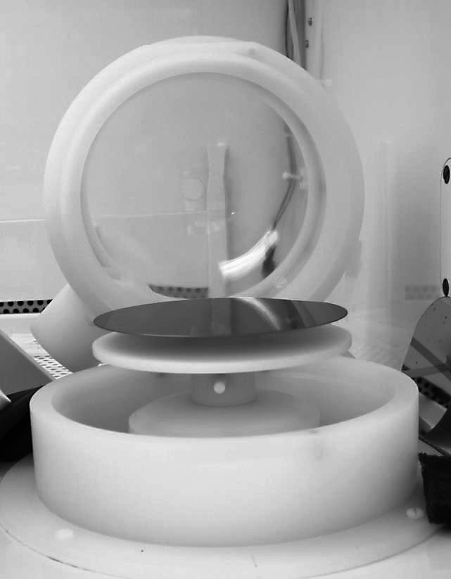
Spin coating is a procedure used to deposit uniform thin films onto flat substrates. Usually a small amount of coating material in liquid form is applied on the center of the substrate, which is either spinning at low speed or not spinning at all. The substrate is then rotated at speeds up to 10,000 rpm to spread the coating material by centrifugal force. A machine used for spin coating is called a spin coater, or simply spinner. Rotation is continued while the fluid spins off the edges of the substrate, until the desired thickness of the film is achieved. The applied solvent is usually volatile, and simultaneously evaporates. The higher the angular speed of spinning, the thinner the film. The thickness of the film also depends on the viscosity and concentration of the solution, and the solvent. Pioneering theoretical analysis of spin coating was undertaken by Emslie et al., and has been extended by many subsequent authors (including Wilson et al., who studied the rate of sprea ... [...More Info...] [...Related Items...] OR: [Wikipedia] [Google] [Baidu] |
Stencil
Stencilling produces an image or pattern on a surface by applying pigment to a surface through an intermediate object, with designed holes in the intermediate object. The holes allow the pigment to reach only some parts of the surface creating the design. The stencil is both the resulting image or pattern and the intermediate object; the context in which ''stencil'' is used makes clear which meaning is intended. In practice, the (object) stencil is usually a thin sheet of material, such as paper, plastic, wood or metal, with lettering, letters or a design cut from it, used to produce the letters or design on an underlying surface by applying pigment through the cut-out holes in the material. The key advantage of a stencil is that it can be reused to repeatedly and rapidly produce the same letters or design. Although aerosol paint, aerosol or painting stencils can be made for one-time use, typically they are made with the intention of being reused. To be reusable, they must rem ... [...More Info...] [...Related Items...] OR: [Wikipedia] [Google] [Baidu] |
Dip-Pen Nanolithography
Dip pen nanolithography (DPN) is a scanning probe lithography technique where an atomic force microscope (AFM) tip is used to directly create patterns on a substrate. It can be done on a range of substances with a variety of inks. A common example of this technique is exemplified by the use of alkane thiolates to imprint onto a gold surface. This technique allows surface patterning on scales of under 100 nanometers. DPN is the nanotechnology analog of the dip pen (also called the quill pen), where the tip of an atomic force microscope cantilever acts as a "pen", which is coated with a chemical compound or mixture acting as an "ink", and put in contact with a substrate, the "paper". DPN enables direct deposition of nanoscale materials onto a substrate in a flexible manner. Recent advances have demonstrated massively parallel patterning using two-dimensional arrays of 55,000 tips. Applications of this technology currently range through chemistry, materials science, and t ... [...More Info...] [...Related Items...] OR: [Wikipedia] [Google] [Baidu] |
Soft Lithography
In technology, soft lithography is a family of techniques for fabricating or Replication (other), replicating structures using "elastomeric stamps, molds, and conformable photomasks". It is called "soft" because it uses elastomeric materials, most notably Polydimethylsiloxane, PDMS. Soft lithography is generally used to construct features measured on the micrometer to nanometer Scale (measurement), scale. According to Rogers and Nuzzo (2005), Research and development, development of soft lithography expanded rapidly from 1995 to 2005. Soft lithography tools are now commercially available. Types * PDMS stamp * Microcontact printing * Multilayer soft lithography * Nanosphere lithography * Patterning by etching at the nanoscale Advantages Soft lithography has some unique advantages over other forms of lithography (such as photolithography and electron beam lithography). They include the following: *Lower cost than traditional photolithography in mass production *Well- ... [...More Info...] [...Related Items...] OR: [Wikipedia] [Google] [Baidu] |
Electron Beam Lithography
Electron-beam lithography (often abbreviated as e-beam lithography or EBL) is the practice of scanning a focused beam of electrons to draw custom shapes on a surface covered with an electron-sensitive film called a resist (exposing). The electron beam changes the solubility of the resist, enabling selective removal of either the exposed or non-exposed regions of the resist by immersing it in a solvent (developing). The purpose, as with photolithography, is to create very small structures in the resist that can subsequently be transferred to the substrate material, often by etching. The primary advantage of electron-beam lithography is that it can draw custom patterns (direct-write) with sub-10 nm resolution. This form of maskless lithography has high resolution but low throughput, limiting its usage to photomask fabrication, low-volume production of semiconductor devices, and research and development. Systems Electron-beam lithography systems used in commercial application ... [...More Info...] [...Related Items...] OR: [Wikipedia] [Google] [Baidu] |
Scanning Electron Microscope
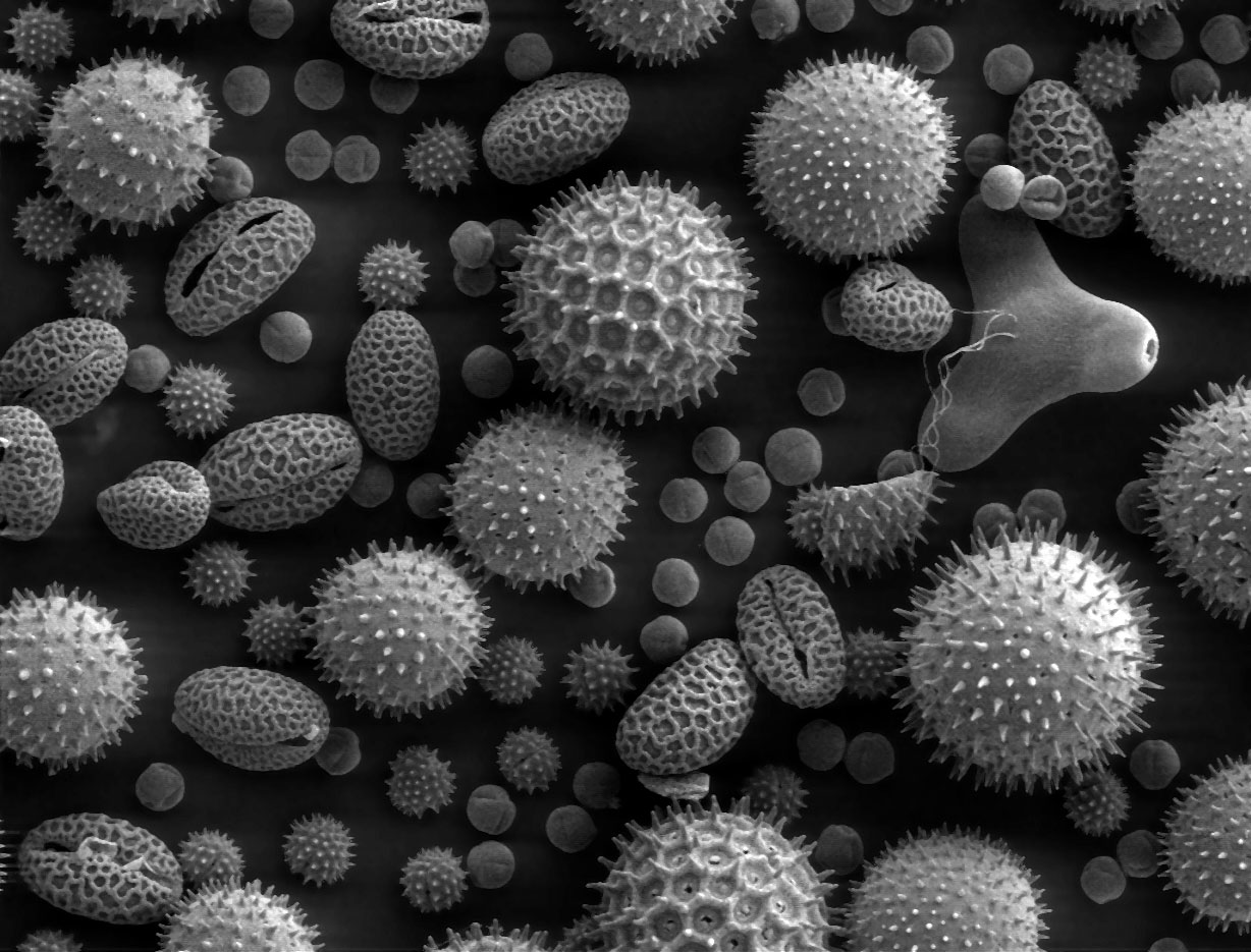
A scanning electron microscope (SEM) is a type of electron microscope that produces images of a sample by scanning the surface with a focused beam of electrons. The electrons interact with atoms in the sample, producing various signals that contain information about the surface topography and composition. The electron beam is scanned in a raster scan pattern, and the position of the beam is combined with the intensity of the detected signal to produce an image. In the most common SEM mode, secondary electrons emitted by atoms excited by the electron beam are detected using a secondary electron detector ( Everhart–Thornley detector). The number of secondary electrons that can be detected, and thus the signal intensity, depends, among other things, on specimen topography. Some SEMs can achieve resolutions better than 1 nanometer. Specimens are observed in high vacuum in a conventional SEM, or in low vacuum or wet conditions in a variable pressure or environmental SEM, an ... [...More Info...] [...Related Items...] OR: [Wikipedia] [Google] [Baidu] |
Electron
The electron (, or in nuclear reactions) is a subatomic particle with a negative one elementary charge, elementary electric charge. It is a fundamental particle that comprises the ordinary matter that makes up the universe, along with up quark, up and down quark, down quarks. Electrons are extremely lightweight particles that orbit the positively charged atomic nucleus, nucleus of atoms. Their negative charge is balanced by the positive charge of protons in the nucleus, giving atoms their overall electric charge#Charge neutrality, neutral charge. Ordinary matter is composed of atoms, each consisting of a positively charged nucleus surrounded by a number of orbiting electrons equal to the number of protons. The configuration and energy levels of these orbiting electrons determine the chemical properties of an atom. Electrons are bound to the nucleus to different degrees. The outermost or valence electron, valence electrons are the least tightly bound and are responsible for th ... [...More Info...] [...Related Items...] OR: [Wikipedia] [Google] [Baidu] |


