|
Physical Design (electronics)
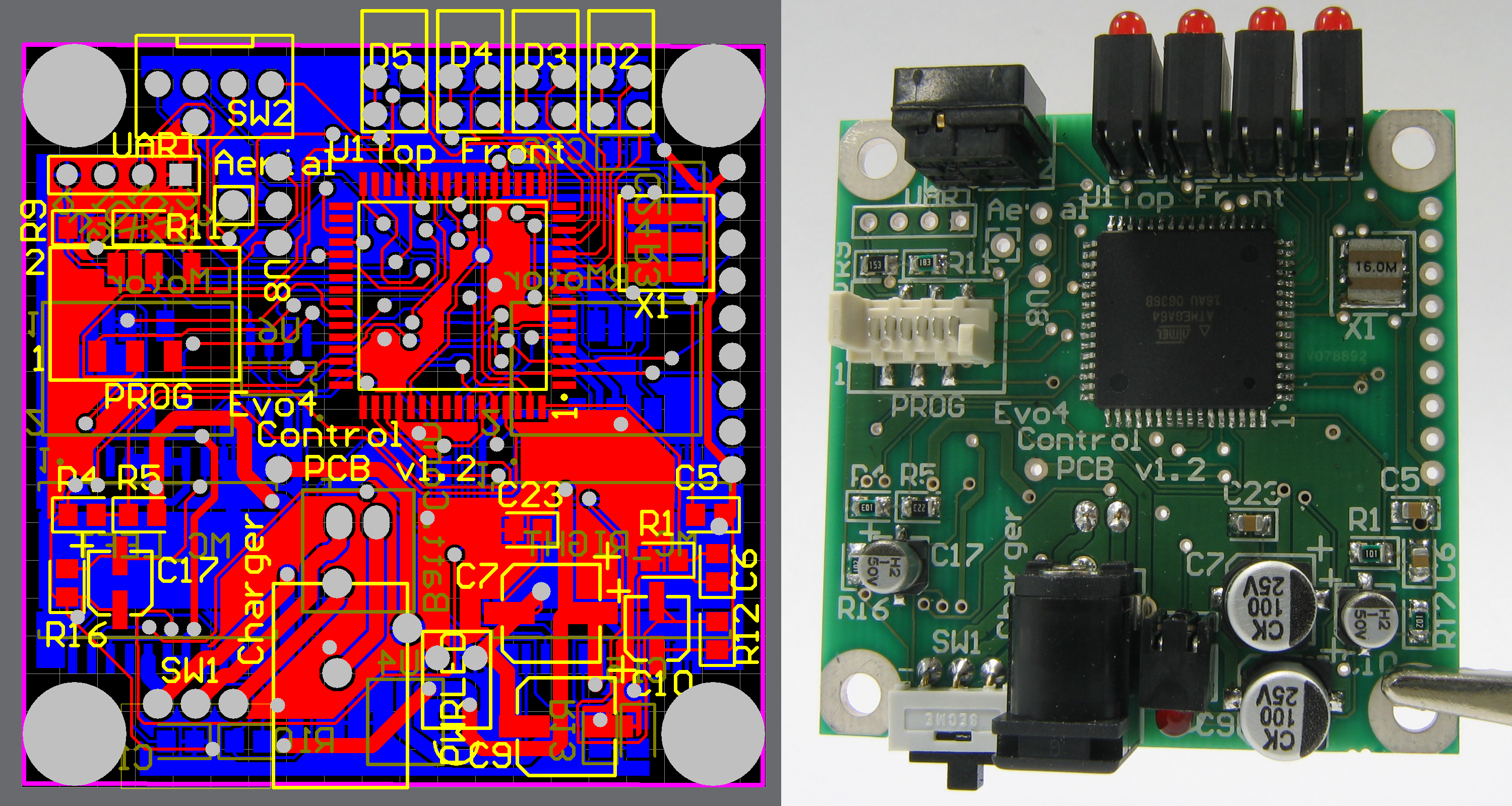
In integrated circuit design, physical design is a step in the standard design cycle which follows after the circuit design. At this step, circuit representations of the components (devices and interconnects) of the design are converted into geometric representations of shapes which, when manufactured in the corresponding layers of materials, will ensure the required functioning of the components. This geometric representation is called integrated circuit layout. This step is usually split into several sub-steps, which include both design and verification and validation of the layout. Modern day Integrated Circuit (IC) design is split up into ''Front-end Design using HDLs'' and ''Back-end Design'' or ''Physical Design''. The inputs to physical design are (i) a netlist, (ii) library information on the basic devices in the design, and (iii) a technology file containing the manufacturing constraints. Physical design is usually concluded by ''Layout Post Processing'', in which amend ... [...More Info...] [...Related Items...] OR: [Wikipedia] [Google] [Baidu] |
Micrometre
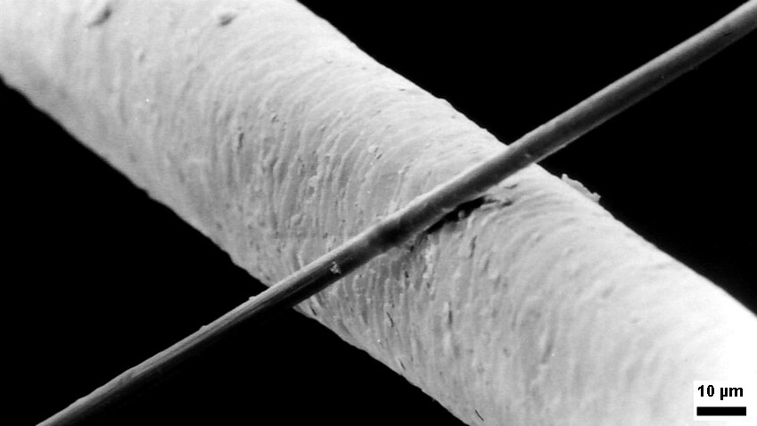
The micrometre (English in the Commonwealth of Nations, Commonwealth English as used by the International Bureau of Weights and Measures; SI symbol: μm) or micrometer (American English), also commonly known by the non-SI term micron, is a unit of length in the International System of Units (SI) equalling (SI standard prefix "micro-" = ); that is, one millionth of a metre (or one thousandth of a millimetre, , or about ). The nearest smaller common SI Unit, SI unit is the nanometre, equivalent to one thousandth of a micrometre, one millionth of a millimetre or one billionth of a metre (). The micrometre is a common unit of measurement for wavelengths of infrared radiation as well as sizes of biological cell (biology), cells and bacteria, and for grading wool by the diameter of the fibres. The width of a single human hair ranges from approximately 20 to . Examples Between 1 μm and 10 μm: * 1–10 μm – length of a typical bacterium * 3–8 μm – width of str ... [...More Info...] [...Related Items...] OR: [Wikipedia] [Google] [Baidu] |
Front End Of Line
The front end of line (FEOL) is the first portion of IC fabrication where the individual components (transistors, capacitors, resistors, etc.) are patterned in a semiconductor substrate. FEOL generally covers everything up to (but not including) the deposition of metal interconnect layers. Steps For the CMOS process, FEOL contains all fabrication steps needed to form isolated CMOS elements: # Selecting the type of wafer to be used; Chemical-mechanical planarization (CMP) and cleaning of the wafer. # Shallow trench isolation (STI) (or LOCOS in early processes with feature size > 0.25 μm); # Well formation; # Gate module formation; # Source and drain module formation. Finally, the surface is treated to prepare the contacts for the subsequent metallization. This concludes the FEOL process, that is, all devices have been built. Following these steps, the devices must be connected electrically as per the nets to build the electrical circuit. This is done in the back end of l ... [...More Info...] [...Related Items...] OR: [Wikipedia] [Google] [Baidu] |
Resolution Enhancement Technologies
Resolution enhancement technologies are methods used to modify the photomasks in the lithographic processes used to make integrated circuits (ICs or "chips") to compensate for limitations in the optical resolution of the projection systems. These processes allow the creation of features well beyond the limit that would normally apply due to the Rayleigh criterion. Modern technologies allow the creation of features on the order of 5 nanometers (nm), far below the normal resolution possible using deep ultraviolet (DUV) light. Background Integrated circuits are created in a multi-step process known as photolithography. This process starts with the design of the IC circuitry as a series of layers than will be patterned onto the surface of a sheet of silicon or other semiconductor material known as a wafer. Each layer of the ultimate design is patterned onto a photomask, which in modern systems is made of fine lines of chromium deposited on highly purified quartz glass. Chromium ... [...More Info...] [...Related Items...] OR: [Wikipedia] [Google] [Baidu] |
Photomask
A photomask (also simply called a mask) is an opaque plate with transparent areas that allow light to shine through in a defined pattern. Photomasks are commonly used in photolithography for the production of integrated circuits (ICs or "chips") to produce a pattern on a thin wafer of material (usually silicon). In semiconductor manufacturing, a mask is sometimes called a reticle. In photolithography, several masks are used in turn, each one reproducing a layer of the completed design, and together known as a mask set. A curvilinear photomask has patterns with curves, which is a departure from conventional photomasks which only have patterns that are completely vertical or horizontal, known as manhattan geometry. These photomasks require special equipment to manufacture. History For IC production in the 1960s and early 1970s, an opaque rubylith film laminated onto a transparent mylar sheet was used. The design of one layer was cut into the rubylith, initially by hand on an i ... [...More Info...] [...Related Items...] OR: [Wikipedia] [Google] [Baidu] |
Mask Data Preparation
A mask is an object normally worn on the face, typically for protection, disguise, performance, or entertainment, and often employed for rituals and rites. Masks have been used since antiquity for both ceremonial and practical purposes, as well as in the performing arts and for entertainment. They are usually worn on the face, although they may also be positioned for effect elsewhere on the wearer's body. In art history, especially sculpture, "mask" is the term for a face without a body that is not modelled in the round (which would make it a "head"), but for example appears in low relief. Etymology The word "mask" appeared in English in the 1530s, from Middle French ''masque'' "covering to hide or guard the face", derived in turn from Italian ''maschera'', from Medieval Latin ''masca'' "mask, specter, nightmare". This word is of uncertain origin, perhaps from Arabic ''maskharah'' مَسْخَرَۃٌ "buffoon", from the verb ''sakhira'' "to ridicule". However, it may a ... [...More Info...] [...Related Items...] OR: [Wikipedia] [Google] [Baidu] |
Routing (EDA)
In electronic design, wire routing, commonly called simply routing, is a step in the design of printed circuit boards (PCBs) and integrated circuits (ICs). It builds on a preceding step, called placement (electronic design automation), placement, which determines the location of each active element of an IC or component on a PCB. After placement, the routing step adds wires needed to properly connect the placed components while obeying all design rules for the IC. Together, the placement and routing steps of IC design are known as place and route. The task of all routers is the same. They are given some pre-existing polygons consisting of pin (electronics), pins (also called terminals) on cells, and optionally some pre-existing wiring called preroutes. Each of these polygons are associated with a net (electronics), net, usually by name or number. The primary task of the router is to create geometries such that all terminals assigned to the same net are connected, no terminals a ... [...More Info...] [...Related Items...] OR: [Wikipedia] [Google] [Baidu] |
Clock After CTS
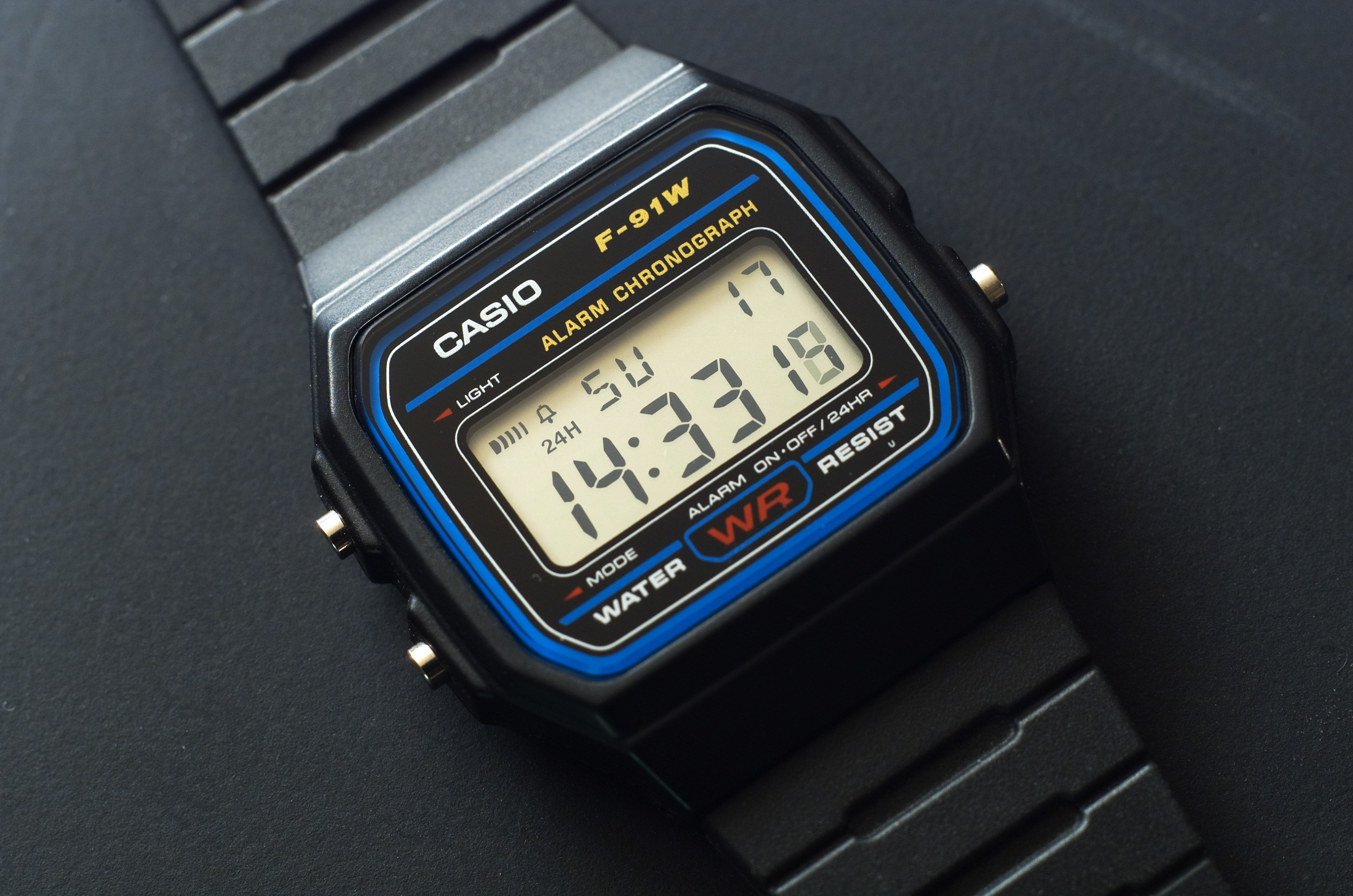
A clock or chronometer is a device that measures and displays time. The clock is one of the oldest Invention, human inventions, meeting the need to measure intervals of time shorter than the natural units such as the day, the lunar month, and the year. Devices operating on several physical processes have been used over the Millennium, millennia. Some predecessors to the modern clock may be considered "clocks" that are based on movement in nature: A sundial shows the time by displaying the position of a shadow on a flat surface. There is a range of duration timers, a well-known example being the hourglass. Water clocks, along with sundials, are possibly the oldest time-measuring instruments. A major advance occurred with the invention of the verge escapement, which made possible the first mechanical clocks around 1300 in Europe, which kept time with oscillating timekeepers like balance wheels., pp. 103–104., p. 31. Traditionally, in horology (the study of timekeeping), the ... [...More Info...] [...Related Items...] OR: [Wikipedia] [Google] [Baidu] |
Ideal Clock
Ideal may refer to: Philosophy * Ideal (ethics), values that one actively pursues as goals * Platonic ideal, a philosophical idea of trueness of form, associated with Plato Mathematics * Ideal (ring theory), special subsets of a ring considered in abstract algebra * Ideal, special subsets of a semigroup * Ideal (order theory), special kind of lower sets of an order * Ideal (set theory), a collection of sets regarded as "small" or "negligible" * Ideal (Lie algebra), a particular subset in a Lie algebra * Ideal point, a boundary point in hyperbolic geometry * Ideal triangle, a triangle in hyperbolic geometry whose vertices are ideal points Science * Ideal chain, in science, the simplest model describing a polymer * Ideal gas law, in physics, governing the pressure of an ideal gas * Ideal transformer, an electrical transformer having zero resistance and perfect magnetic threading * Ideal final result, in TRIZ methodology, the best possible solution * Thought experiment, sometimes ... [...More Info...] [...Related Items...] OR: [Wikipedia] [Google] [Baidu] |
Floorplan (microelectronics)
In electronic design automation, a floorplan of an integrated circuit consists of a schematic arrangement of its major functional blocks on the chip area and the specification of high-level parameters such as the aspect ratio or core utilization. The design step in which floorplans are created is called floorplanning, an early stage in the Design flow (EDA), design flow for integrated circuit design. Various mathematical abstractions of this problem have been studied. Floorplanning design stage The floorplanning design stage consists of various steps with the aim of finding floorplans that allow a Timing closure, timing-clean routing and spread power consumption over the whole chip. *Chip Area Estimation: The dimensions and aspect ratio of the chip area are determined. The estimation considers the space required to place macros, standard cells and I/O ports while also leaving enough space for routing resources to enable a successful Place and route, place and route design fl ... [...More Info...] [...Related Items...] OR: [Wikipedia] [Google] [Baidu] |
Silicon On Insulator
In semiconductor manufacturing, silicon on insulator (SOI) technology is fabrication of silicon semiconductor devices in a layered silicon–insulator–silicon substrate, to reduce parasitic capacitance within the device, thereby improving performance. SOI-based devices differ from conventional silicon-built devices in that the silicon junction is above an electrical insulator, typically silicon dioxide or sapphire (these types of devices are called silicon on sapphire, or SOS). The choice of insulator depends largely on intended application, with sapphire being used for high-performance radio frequency (RF) and radiation-sensitive applications, and silicon dioxide for diminished short-channel effects in other microelectronics devices. The insulating layer and topmost silicon layer also vary widely with application. Industry need SOI technology is one of several manufacturing strategies to allow the continued miniaturization of microelectronic devices, colloquially referred to ... [...More Info...] [...Related Items...] OR: [Wikipedia] [Google] [Baidu] |
Nanometre
330px, Different lengths as in respect to the Molecule">molecular scale. The nanometre (international spelling as used by the International Bureau of Weights and Measures; SI symbol: nm), or nanometer (American spelling), is a unit of length in the International System of Units (SI), equal to one billionth ( short scale) or one thousand million (long scale) of a meter (0.000000001 m) and to 1000 picometres. One nanometre can be expressed in scientific notation as 1 × 10⁻⁹ m and as m. History The nanometre was formerly known as the "''millimicrometre''" – or, more commonly, the "''millimicron''" for short – since it is of a micrometer. It was often denoted by the symbol ''mμ'' or, more rarely, as ''μμ'' (however, ''μμ'' should refer to a ''millionth'' of a micron). Etymology The name combines the SI prefix '' nano-'' (from the Ancient Greek , ', "dwarf") with the parent unit name ''metre'' (from Greek , ', "unit of measurement"). ... [...More Info...] [...Related Items...] OR: [Wikipedia] [Google] [Baidu] |


