|
IC Layout Editor
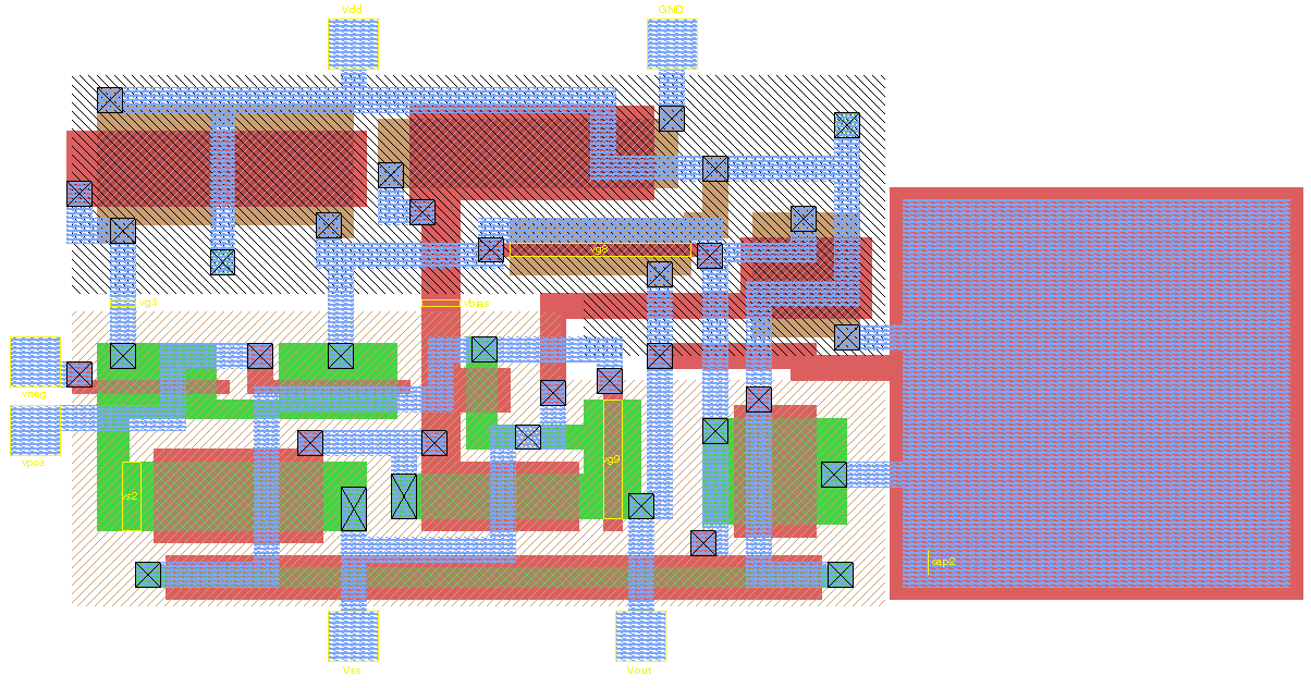
An integrated circuit layout editor or IC layout editor is an electronic design automation software tool that allows a user to digitize the shapes and patterns that form an integrated circuit. Typically the view will include the components (usually as pcells), metal routing tracks, vias and electrical pins. Software of this type is similar to computer aided drafting software, but is specialized for the task of integrated circuit layout. The typical flow for the layout of analog circuits might be : :1. The layout engineer receives the schematic from the designer in electrical form :2. Either the tool or the layout engineer creates a physical view of the circuit including all of the required components, wires, layers and pads. :3. The layout engineer positions the components to minimize both the area required and the negative effects of layout parasitics upon the circuit performance and also to allow efficient routing to components. :4. The layout engineer uses metal routing and ot ... [...More Info...] [...Related Items...] OR: [Wikipedia] [Google] [Baidu] |
Electronic Design Automation
Electronic design automation (EDA), also referred to as electronic computer-aided design (ECAD), is a category of software tools for designing Electronics, electronic systems such as integrated circuits and printed circuit boards. The tools work together in a Design flow (EDA), design flow that chip designers use to design and analyze entire semiconductor chips. Since a modern semiconductor chip can have billions of components, EDA tools are essential for their design; this article in particular describes EDA specifically with respect to integrated circuits (ICs). History Early days The earliest electronic design automation is attributed to IBM with the documentation of its IBM 700/7000 series, 700 series computers in the 1950s. Prior to the development of EDA, integrated circuits were designed by hand and manually laid out. Some advanced shops used geometric software to generate tapes for a Gerber format, Gerber photoplotter, responsible for generating a monochromatic ex ... [...More Info...] [...Related Items...] OR: [Wikipedia] [Google] [Baidu] |
Integrated Circuit
An integrated circuit (IC), also known as a microchip or simply chip, is a set of electronic circuits, consisting of various electronic components (such as transistors, resistors, and capacitors) and their interconnections. These components are etched onto a small, flat piece ("chip") of semiconductor material, usually silicon. Integrated circuits are used in a wide range of electronic devices, including computers, smartphones, and televisions, to perform various functions such as processing and storing information. They have greatly impacted the field of electronics by enabling device miniaturization and enhanced functionality. Integrated circuits are orders of magnitude smaller, faster, and less expensive than those constructed of discrete components, allowing a large transistor count. The IC's mass production capability, reliability, and building-block approach to integrated circuit design have ensured the rapid adoption of standardized ICs in place of designs using discre ... [...More Info...] [...Related Items...] OR: [Wikipedia] [Google] [Baidu] |
Via (electronics)
A via (Latin, 'path' or 'way') is an electrical connection between two or more metal layers of a printed circuit boards (PCB) or integrated circuit. Essentially a via is a small drilled hole that goes through two or more adjacent layers; the hole is plated with metal (often copper) that forms an electrical connection through the insulating layers. Vias are an important concern in PCB manufacturing. As vertical structures crossing multiple layers, they are specified differently from most of the design, which increases the chance for errors. They place the strictest demands on registration (how closely aligned different layers are). They are manufactured with different tooling from other features -- tooling that typically has looser tolerances. If either the hole or any layer is slightly out of place, the wrong electrical connections may be made; this may not be visible from the surface. After the hole is drilled, it must also be lined with conductive material, as opposed to simpl ... [...More Info...] [...Related Items...] OR: [Wikipedia] [Google] [Baidu] |
Computer Aided Drafting
Computer-aided design (CAD) is the use of computers (or ) to aid in the creation, modification, analysis, or optimization of a design. This software is used to increase the productivity of the designer, improve the quality of design, improve communications through documentation, and to create a database for manufacturing. Designs made through CAD software help protect products and inventions when used in patent applications. CAD output is often in the form of electronic files for print, machining, or other manufacturing operations. The terms computer-aided drafting (CAD) and computer-aided design and drafting (CADD) are also used. Its use in designing electronic systems is known as ''electronic design automation'' (''EDA''). In mechanical design it is known as ''mechanical design automation'' (''MDA''), which includes the process of creating a technical drawing with the use of computer software. CAD software for mechanical design uses either vector-based graphics to depict th ... [...More Info...] [...Related Items...] OR: [Wikipedia] [Google] [Baidu] |
Integrated Circuit Layout
In integrated circuit design, integrated circuit (IC) layout, also known IC mask layout or mask design, is the representation of an integrated circuit in terms of planar geometric shapes which correspond to the patterns of metal, oxide, or semiconductor layers that make up the components of the integrated circuit. Originally the overall process was called tapeout, as historically early ICs used graphical black crepe tape on mylar media for photo imaging (erroneously believed to reference magnetic data—the photo process greatly predated magnetic media). When using a standard process—where the interaction of the many chemical, thermal, and photographic variables is known and carefully controlled—the behaviour of the final integrated circuit depends largely on the positions and interconnections of the geometric shapes. Using a computer-aided layout tool, the layout engineer—or layout technician—places and connects all of the components that make up the chip such that ... [...More Info...] [...Related Items...] OR: [Wikipedia] [Google] [Baidu] |
Design Rule Checking
In electronic design automation, a design rule is a geometric constraint imposed on circuit board, semiconductor device, and integrated circuit (IC) designers to ensure their designs function properly, reliably, and can be produced with acceptable yield. Design rules for production are developed by process engineers based on the capability of their processes to realize design intent. Electronic design automation is used extensively to ensure that designers do not violate design rules; a process called design rule checking (DRC). DRC is a major step during physical verification signoff on the design, which also involves LVS ( layout versus schematic) checks, XOR checks, ERC (electrical rule check), and antenna checks. The importance of design rules and DRC is greatest for ICs, which have micro- or nano-scale geometries; for advanced processes, some fabs also insist upon the use of more restricted rules to improve yield. Design rules Design rules are a series of parameters provi ... [...More Info...] [...Related Items...] OR: [Wikipedia] [Google] [Baidu] |
Parasitic Capacitance
Parasitic capacitance or stray capacitance is the unavoidable and usually unwanted capacitance that exists between the parts of an electronic component or circuit simply because of their proximity to each other. When two electrical conductors at different voltages are close together, the electric field between them causes electric charge to be stored on them; this effect is capacitance. All practical circuit elements such as inductors, diodes, and transistors have internal capacitance, which can cause their behavior to depart from that of ideal circuit elements. Additionally, there is always some capacitance between any two conductors; this can be significant with closely spaced conductors, such as adjacent wires or printed circuit board traces. The parasitic capacitance between the turns of an inductor (e.g. Figure 1) or other wound component is often described as ''self-capacitance''. However, in electromagnetics, the term self-capacitance more correctly refers to a diffe ... [...More Info...] [...Related Items...] OR: [Wikipedia] [Google] [Baidu] |


