|
Heterojunction Bipolar Transistor
A heterojunction bipolar transistor (HBT) is a type of bipolar junction transistor (BJT) that uses different semiconductor materials for the emitter and base regions, creating a heterojunction. The HBT improves on the BJT in that it can handle signals of very high frequencies, up to several hundred GHz. It is commonly used in modern ultrafast circuits, mostly radio frequency (RF) systems, and in applications requiring a high power efficiency, such as RF power amplifiers in cellular phones. The idea of employing a heterojunction is as old as the conventional BJT, dating back to a patent from 1951. Detailed theory of heterojunction bipolar transistor was developed by Herbert Kroemer in 1957. Materials The principal difference between the BJT and HBT is in the use of differing semiconductor materials for the emitter-base junction and the base-collector junction, creating a heterojunction. The effect is to limit the injection of holes from the base into the emitter region, since ... [...More Info...] [...Related Items...] OR: [Wikipedia] [Google] [Baidu] |
Bipolar Junction Transistor
A bipolar junction transistor (BJT) is a type of transistor that uses both electrons and electron holes as charge carriers. In contrast, a unipolar transistor, such as a field-effect transistor (FET), uses only one kind of charge carrier. A bipolar transistor allows a small current injected at one of its terminals to control a much larger current between the remaining two terminals, making the device capable of amplification or switching. BJTs use two p–n junctions between two semiconductor types, n-type and p-type, which are regions in a single crystal of material. The junctions can be made in several different ways, such as changing the doping of the semiconductor material as it is grown, by depositing metal pellets to form alloy junctions, or by such methods as diffusion of n-type and p-type doping substances into the crystal. The superior predictability and performance of junction transistors quickly displaced the original point-contact transistor. Diffused trans ... [...More Info...] [...Related Items...] OR: [Wikipedia] [Google] [Baidu] |
Indium Gallium Nitride
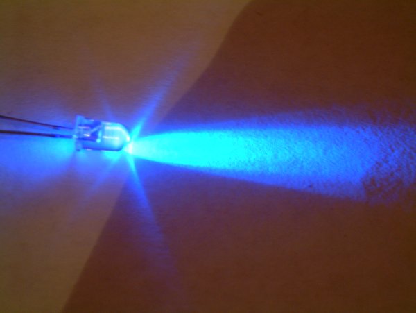
Indium gallium nitride (InGaN, ) is a semiconductor material made of a mix of gallium nitride (GaN) and indium nitride (InN). It is a ternary group III/ group V direct bandgap semiconductor. Its bandgap can be tuned by varying the amount of indium in the alloy. InxGa1−xN has a direct bandgap span from the infrared (0.69 eV) for InN to the ultraviolet (3.4 eV) of GaN. The ratio of In/Ga is usually between 0.02/0.98 and 0.3/0.7. Applications LEDs Indium gallium nitride is the light-emitting layer in modern blue and green LEDs and often grown on a GaN buffer on a transparent substrate as, e.g. sapphire or silicon carbide. It has a high heat capacity and its sensitivity to ionizing radiation is low (like other group III nitrides), making it also a potentially suitable material for solar photovoltaic devices, specifically for arrays for satellites. It is theoretically predicted that spinodal decomposition of indium nitride should occur for compositions between 15% and 85%, ... [...More Info...] [...Related Items...] OR: [Wikipedia] [Google] [Baidu] |
Microwave Technology
Microwave is a form of electromagnetic radiation with wavelengths shorter than other radio waves but longer than infrared waves. Its wavelength ranges from about one meter to one millimeter, corresponding to frequency, frequencies between 300 MHz and 300 GHz, broadly construed. A more common definition in radio-frequency engineering is the range between 1 and 100 GHz (wavelengths between 30 cm and 3 mm), or between 1 and 3000 GHz (30 cm and 0.1 mm). In all cases, microwaves include the entire super high frequency, super high frequency (SHF) band (3 to 30 GHz, or 10 to 1 cm) at minimum. The boundaries between far infrared, terahertz radiation, microwaves, and ultra-high-frequency (UHF) are fairly arbitrary and differ between different fields of study. The prefix ' in ''microwave'' indicates that microwaves are small (having shorter wavelengths), compared to the radio waves used in prior radio technology. Frequencies in the micr ... [...More Info...] [...Related Items...] OR: [Wikipedia] [Google] [Baidu] |
MESFET
A MESFET (metal–semiconductor field-effect transistor) is a field-effect transistor semiconductor device similar to a JFET with a Schottky (metal–semiconductor) junction instead of a p–n junction for a gate. Construction MESFETs are constructed in compound semiconductor technologies lacking high quality surface passivation, such as gallium arsenide, indium phosphide, or silicon carbide, and are faster but more expensive than silicon-based JFETs or MOSFETs. Production MESFETs are operated up to approximately 45 GHz, and are commonly used for microwave frequency communications and radar. The first MESFETs were developed in 1966, and a year later their extremely high frequency RF microwave performance was demonstrated. radio-electronics.com. Funct ...
|
High-electron-mobility Transistor
A high-electron-mobility transistor (HEMT or HEM FET), also known as heterostructure FET (HFET) or modulation-doped FET (MODFET), is a field-effect transistor incorporating a junction between two materials with different band gaps (i.e. a heterojunction) as the channel instead of a doped region (as is generally the case for a MOSFET). A commonly used material combination is Gallium arsenide, GaAs with Aluminium gallium arsenide, AlGaAs, though there is wide variation, dependent on the application of the device. Devices incorporating more indium generally show better high-frequency performance, while in recent years, gallium nitride HEMTs have attracted attention due to their high-power performance. Like other FETs, HEMTs can be used in integrated circuits as digital on-off switches. FETs can also be used as amplifiers for large amounts of current using a small voltage as a control signal. Both of these uses are made possible by the FET’s unique current–voltage characteristic ... [...More Info...] [...Related Items...] OR: [Wikipedia] [Google] [Baidu] |
Wavelength
In physics and mathematics, wavelength or spatial period of a wave or periodic function is the distance over which the wave's shape repeats. In other words, it is the distance between consecutive corresponding points of the same ''phase (waves), phase'' on the wave, such as two adjacent crests, troughs, or zero crossings. Wavelength is a characteristic of both traveling waves and standing waves, as well as other spatial wave patterns. The multiplicative inverse, inverse of the wavelength is called the ''spatial frequency''. Wavelength is commonly designated by the Greek letter lambda (''λ''). For a modulated wave, ''wavelength'' may refer to the carrier wavelength of the signal. The term ''wavelength'' may also apply to the repeating envelope (mathematics), envelope of modulated waves or waves formed by Interference (wave propagation), interference of several sinusoids. Assuming a sinusoidal wave moving at a fixed phase velocity, wave speed, wavelength is inversely proportion ... [...More Info...] [...Related Items...] OR: [Wikipedia] [Google] [Baidu] |
University Of Illinois At Urbana-Champaign
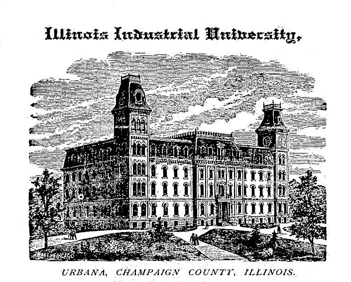
The University of Illinois Urbana-Champaign (UIUC, U of I, Illinois, or University of Illinois) is a public land-grant research university in the Champaign–Urbana metropolitan area, Illinois, United States. Established in 1867, it is the founding campus and flagship institution of the University of Illinois System. With over 59,000 students, the University of Illinois is one of the largest public universities by enrollment in the United States. The university contains 16 schools and colleges and offers more than 150 undergraduate and over 100 graduate programs of study. The university holds 651 buildings on and its annual operating budget in 2016 was over $2 billion. The University of Illinois Urbana-Champaign also operates a research park home to innovation centers for over 90 start-up companies and multinational corporations. The University of Illinois Urbana-Champaign is a member of the Association of American Universities and is classified among "R1: Doctoral Univ ... [...More Info...] [...Related Items...] OR: [Wikipedia] [Google] [Baidu] |
III-V
Semiconductor materials are nominally small band gap insulators. The defining property of a semiconductor material is that it can be compromised by doping it with impurities that alter its electronic properties in a controllable way. Because of their application in the computer and photovoltaic industry—in devices such as transistors, lasers, and solar cells—the search for new semiconductor materials and the improvement of existing materials is an important field of study in materials science. Most commonly used semiconductor materials are crystalline inorganic solids. These materials are classified according to the periodic table groups of their constituent atoms. Different semiconductor materials differ in their properties. Thus, in comparison with silicon, compound semiconductors have both advantages and disadvantages. For example, gallium arsenide (GaAs) has six times higher electron mobility than silicon, which allows faster operation; wider band gap, which allows ... [...More Info...] [...Related Items...] OR: [Wikipedia] [Google] [Baidu] |
MOVPE
Metalorganic vapour-phase epitaxy (MOVPE), also known as organometallic vapour-phase epitaxy (OMVPE) or metalorganic chemical vapour deposition (MOCVD), is a chemical vapour deposition method used to produce single- or polycrystalline thin films. It is a process for growing crystalline layers to create complex semiconductor multilayer structures. In contrast to molecular-beam epitaxy (MBE), the growth of crystals is by chemical reaction and not physical deposition. This takes place not in vacuum, but from the gas phase at moderate pressures (10 to 760 Torr). As such, this technique is preferred for the formation of devices incorporating thermodynamically metastable alloys, and it has become a major process in the manufacture of optoelectronics, such as light-emitting diodes, its most widespread application. It was first demonstrated in 1967 at North American Aviation (later Rockwell International) Autonetics Division in Anaheim CA by Harold M. Manasevit. Basic principl ... [...More Info...] [...Related Items...] OR: [Wikipedia] [Google] [Baidu] |
Chemical Vapor Deposition
Chemical vapor deposition (CVD) is a vacuum deposition method used to produce high-quality, and high-performance, solid materials. The process is often used in the semiconductor industry to produce thin films. In typical CVD, the wafer (electronics), wafer (substrate) is exposed to one or more Volatility (chemistry), volatile wikt:precursor, precursors, which chemical reaction, react and/or chemical decomposition, decompose on the substrate surface to produce the desired deposit. Frequently, volatile by-products are also produced, which are removed by gas flow through the reaction chamber. Microfabrication processes widely use CVD to deposit materials in various forms, including: Single crystal, monocrystalline, polycrystalline, amorphous, and Epitaxy, epitaxial. These materials include: silicon (Silicon dioxide, dioxide, silicon carbide, carbide, silicon nitride, nitride, silicon oxynitride, oxynitride), carbon (carbon (fiber), fiber, carbon nanofibers, nanofibers, carbon nanot ... [...More Info...] [...Related Items...] OR: [Wikipedia] [Google] [Baidu] |
Photolithography
Photolithography (also known as optical lithography) is a process used in the manufacturing of integrated circuits. It involves using light to transfer a pattern onto a substrate, typically a silicon wafer. The process begins with a photosensitive material, called a photoresist, being applied to the substrate. A photomask that contains the desired pattern is then placed over the photoresist. Light is shone through the photomask, exposing the photoresist in certain areas. The exposed areas undergo a chemical change, making them either soluble or insoluble in a developer solution. After development, the pattern is transferred onto the substrate through etching, chemical vapor deposition, or ion implantation processes. Ultraviolet, Ultraviolet (UV) light is typically used. Photolithography processes can be classified according to the type of light used, including ultraviolet lithography, deep ultraviolet lithography, extreme ultraviolet lithography, extreme ultraviolet lithography ... [...More Info...] [...Related Items...] OR: [Wikipedia] [Google] [Baidu] |
Ohmic Contact
An ohmic contact is a non- rectifying electrical junction: a junction between two conductors that has a linear current–voltage (I–V) curve as with Ohm's law Ohm's law states that the electric current through a Electrical conductor, conductor between two Node (circuits), points is directly Proportionality (mathematics), proportional to the voltage across the two points. Introducing the constant of .... Low-resistance ohmic contacts are used to allow charge to flow easily in both directions between the two conductors, without blocking due to rectification or excess power dissipation due to voltage thresholds. By contrast, a junction or contact that does not demonstrate a linear I–V curve is called non-ohmic. Non-ohmic contacts come in a number of forms, such as p–n junction, Schottky barrier, rectifying heterojunction, or avalanche breakdown, breakdown junction. Generally the term "ohmic contact" implicitly refers to an ohmic contact of a metal to a semiconductor, w ... [...More Info...] [...Related Items...] OR: [Wikipedia] [Google] [Baidu] |


