|
Austrian Centre For Electron Microscopy And Nanoanalysis
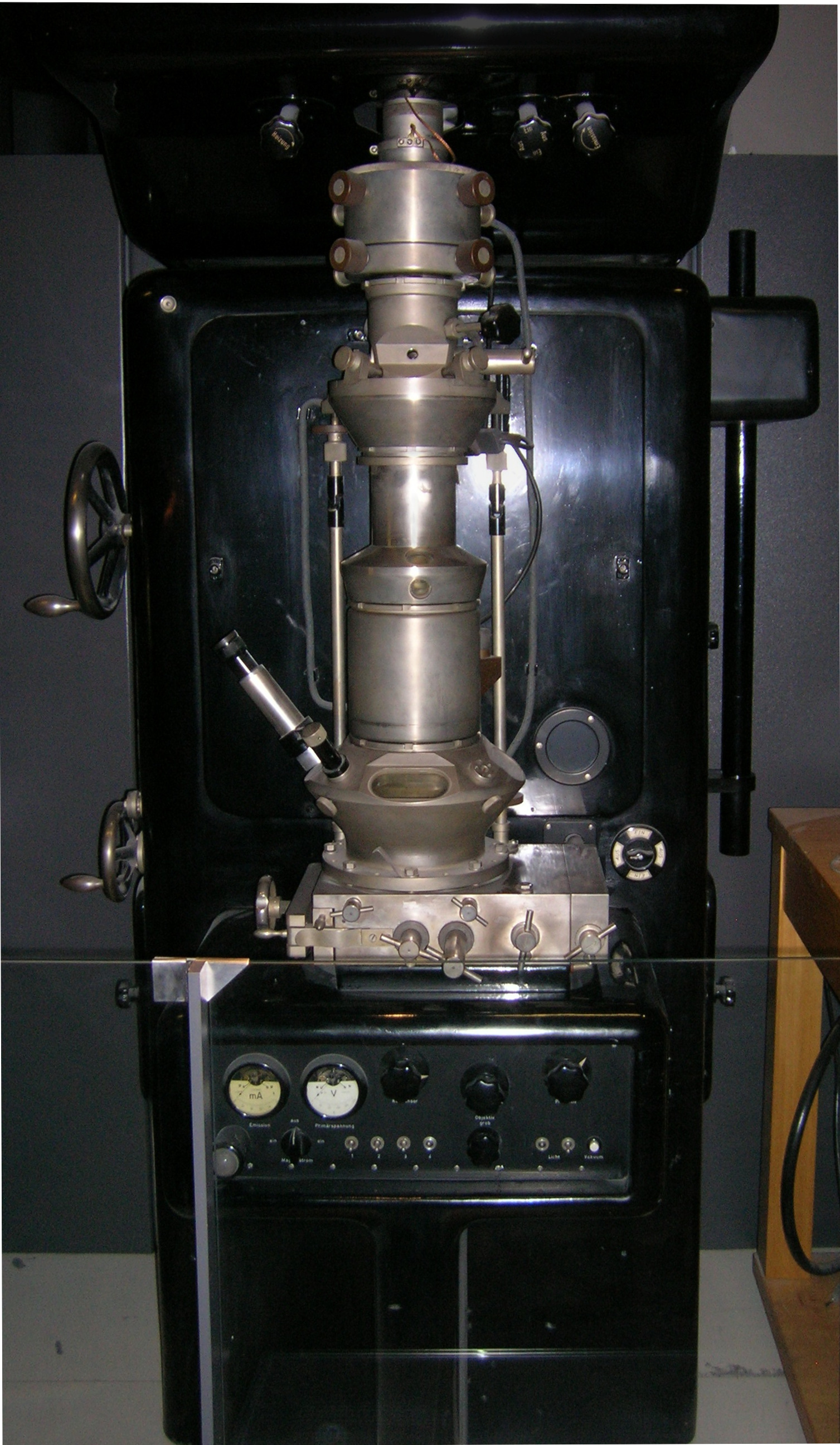
The Austrian Centre for Electron Microscopy and Nanoanalysis (short: FELMI-ZFE) is a cooperation between the Institute of Electron Microscopy and Nanoanalysis (FELMI) of the Graz University of Technology (TUG) and the Graz Centre for Electron Microscopy (ZFE), which is a member of Austrian Cooperative Research (ACR) and run by the non-profit association for the promotion of electron microscopy. It is located at the “Neue Technik Steyrergasse” campus in Graz. The FELMI-ZFE is offering both research and services, to interested partners from academia and industry, using advanced electron microscopic methods for both structural and chemical characterization. History The acquisition process of the first electron microscope of the Graz University of Technology was started by a donation from industry in 1949. The next year a research group, headed by Fritz Grasenick, was established. Finally, the first electron microscope (“Übermikroskop UEM100” by Siemens & Halske) was boug ... [...More Info...] [...Related Items...] OR: [Wikipedia] [Google] [Baidu] |
Graz University Of Technology
Graz University of Technology (, short TU Graz) is a public research university located in Styria, Austria. It was founded in 1811 by Archduke John of Austria and is the oldest science and technology research and educational institute in Austria. It currently comprises seven faculties and is a public university. It offers 19 bachelor's and 36 master's study programmes (of which 20 are in English) across all technology and natural sciences disciplines. Doctoral training is organised in 14 English-speaking doctoral schools. The university has more than 17,000 students, and around 1,900 students graduate every year. The Graz University of Technology and the University of Graz co-operate in teaching and research of natural sciences. The university has a staff of 3,935. Research areas are combined in five fields of expertise. ''TU Graz'', the ''University of Leoben'' and '' TU Wien'' form the network ''Austrian Universities of Technology ( TU Austria)'' with more than 45,000 students ... [...More Info...] [...Related Items...] OR: [Wikipedia] [Google] [Baidu] |
Graz
Graz () is the capital of the Austrian Federal states of Austria, federal state of Styria and the List of cities and towns in Austria, second-largest city in Austria, after Vienna. On 1 January 2025, Graz had a population of 306,068 (343,461 including secondary residence). In 2023, the population of the Graz larger urban zone (LUZ) stood at 660,238. Graz is known as a city of higher education, with four colleges and four universities. Combined, the city is home to more than 60,000 students. Its historic centre (''Altstadt'') is one of the best-preserved city centres in Central Europe. In 1999, the city's historic centre was added to the UNESCO list of World Heritage Sites and in 2010 the designation was expanded to include Eggenberg Palace, Graz, Eggenberg Palace () on the western edge of the city. Graz was designated the Cultural Capital of Europe in 2003 and became a City of Culinary Delights in 2008. In addition, the city is recognized as a "Design Cities (UNESCO), Design City ... [...More Info...] [...Related Items...] OR: [Wikipedia] [Google] [Baidu] |
Ernst Ruska
Ernst August Friedrich Ruska (; 25 December 1906 – 27 May 1988) was a German physicist who won the Nobel Prize in Physics in 1986 for his work in electron optics, including the design of the first electron microscope. Life and career Ernst Ruska was born in Heidelberg, Germany. He was educated at the Technical University of Munich from 1925 to 1927 and then entered ''Technische Hochschule Berlin'' (now Technische Universität Berlin), where he posited that microscopes using electrons, with wavelengths 1000 times shorter than those of light, could provide a more detailed picture of an object than a microscope utilizing light, in which magnification is limited by the size of the wavelengths. In 1931, he demonstrated that a magnetic coil could act as an electron lens, and used several coils in a series to build the first electron microscope in 1933. After completing his PhD in 1933, Ruska continued to work in the field of electron optics, first at Fernseh AG in Berlin-Zehlendo ... [...More Info...] [...Related Items...] OR: [Wikipedia] [Google] [Baidu] |
Scanning Electron Microscope
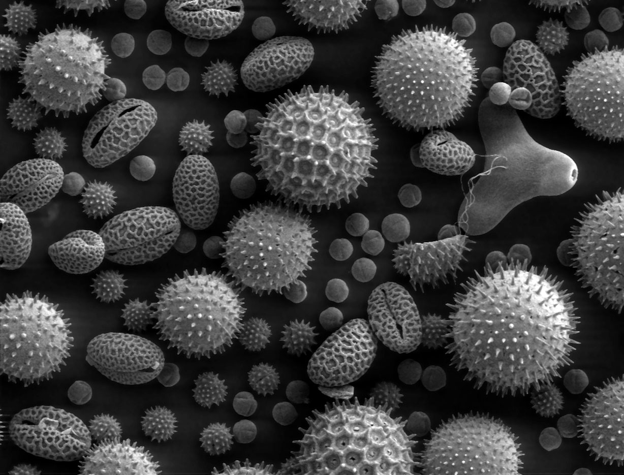
A scanning electron microscope (SEM) is a type of electron microscope that produces images of a sample by scanning the surface with a focused beam of electrons. The electrons interact with atoms in the sample, producing various signals that contain information about the surface topography and composition. The electron beam is scanned in a raster scan pattern, and the position of the beam is combined with the intensity of the detected signal to produce an image. In the most common SEM mode, secondary electrons emitted by atoms excited by the electron beam are detected using a secondary electron detector ( Everhart–Thornley detector). The number of secondary electrons that can be detected, and thus the signal intensity, depends, among other things, on specimen topography. Some SEMs can achieve resolutions better than 1 nanometer. Specimens are observed in high vacuum in a conventional SEM, or in low vacuum or wet conditions in a variable pressure or environmental SEM, an ... [...More Info...] [...Related Items...] OR: [Wikipedia] [Google] [Baidu] |
Transmission Electron Microscopy
Transmission electron microscopy (TEM) is a microscopy technique in which a beam of electrons is transmitted through a specimen to form an image. The specimen is most often an ultrathin section less than 100 nm thick or a suspension on a grid. An image is formed from the interaction of the electrons with the sample as the beam is transmitted through the specimen. The image is then magnified and focused onto an imaging device, such as a fluorescent screen, a layer of photographic film, or a detector such as a scintillator attached to a charge-coupled device or a direct electron detector. Transmission electron microscopes are capable of imaging at a significantly higher resolution than light microscopes, owing to the smaller de Broglie wavelength of electrons. This enables the instrument to capture fine detail—even as small as a single column of atoms, which is thousands of times smaller than a resolvable object seen in a light microscope. Transmission electron micr ... [...More Info...] [...Related Items...] OR: [Wikipedia] [Google] [Baidu] |
Infrared Spectroscopy
Infrared spectroscopy (IR spectroscopy or vibrational spectroscopy) is the measurement of the interaction of infrared radiation with matter by absorption, emission, or reflection. It is used to study and identify chemical substances or functional groups in solid, liquid, or gaseous forms. It can be used to characterize new materials or identify and verify known and unknown samples. The method or technique of infrared spectroscopy is conducted with an instrument called an infrared spectrometer (or spectrophotometer) which produces an infrared spectrum. An IR spectrum can be visualized in a graph of infrared light absorbance (or transmittance) on the vertical axis vs. frequency, wavenumber or wavelength on the horizontal axis. Typical units of wavenumber used in IR spectra are reciprocal centimeters, with the symbol cm−1. Units of IR wavelength are commonly given in micrometers (formerly called "microns"), symbol μm, which are related to the wavenumber in a reciprocal way ... [...More Info...] [...Related Items...] OR: [Wikipedia] [Google] [Baidu] |
Raman Microscope
The Raman microscope is a laser-based microscopic device used to perform Raman spectroscopy.''Microscopical techniques in the use of the molecular optics laser examiner Raman microprobe'', by M. E. Andersen, R. Z. Muggli, Analytical Chemistry, 1981, 53 (12), pp 1772–177/ref> The term MOLE (molecular optics laser examiner) is used to refer to the Raman-based microprobe. The technique used is named after C. V. Raman, who discovered the scattering properties in liquids. Configuration The Raman microscope begins with a standard optical microscope, and adds an excitation laser, laser rejection filters, a spectrometer or monochromator, and an optical sensitive detector such as a charge-coupled device (CCD), or photomultiplier tube, (PMT). Traditionally Raman microscopy was used to measure the Raman spectrum of a point on a sample, more recently the technique has been extended to implement Raman spectroscopy for direct chemical imaging over the whole field of view on a 3D sample. ... [...More Info...] [...Related Items...] OR: [Wikipedia] [Google] [Baidu] |
Focused Ion Beam
Focused ion beam, also known as FIB, is a technique used particularly in the semiconductor industry, materials science and increasingly in the biological field for site-specific analysis, deposition, and ablation of materials. A FIB setup is a scientific instrument that resembles a scanning electron microscope (SEM). However, while the SEM uses a focused beam of electrons to image the sample in the chamber, a FIB setup uses a focused beam of ions instead. FIB can also be incorporated in a system with both electron and ion beam columns, allowing the same feature to be investigated using either of the beams. FIB should not be confused with using a beam of focused ions for direct write lithography (such as in proton beam writing). These are generally quite different systems where the material is modified by other mechanisms. Ion beam source Most widespread instruments are using liquid metal ion sources (LMIS), especially gallium ion sources. Ion sources based on elemental gold an ... [...More Info...] [...Related Items...] OR: [Wikipedia] [Google] [Baidu] |
Atomic Force Microscopy
Atomic force microscopy (AFM) or scanning force microscopy (SFM) is a very-high-resolution type of scanning probe microscopy (SPM), with demonstrated resolution on the order of fractions of a nanometer, more than 1000 times better than the optical diffraction limit. Overview Atomic force microscopy (AFM) gathers information by "feeling" or "touching" the surface with a mechanical probe. Piezoelectric elements that facilitate tiny but accurate and precise movements on (electronic) command enable precise scanning. Despite the name, the Atomic Force Microscope does not use the nuclear force. Abilities and spatial resolution The AFM has three major abilities: force measurement, topographic imaging, and manipulation. In force measurement, AFMs can be used to measure the forces between the probe and the sample as a function of their mutual separation. This can be applied to perform force spectroscopy, to measure the mechanical properties of the sample, such as the sample's Youn ... [...More Info...] [...Related Items...] OR: [Wikipedia] [Google] [Baidu] |


